Welcome to Guangzhou Tongsen Electronic Technology Co., LTD. Website!


What are the requirements and specifications for PCB positioning holes?
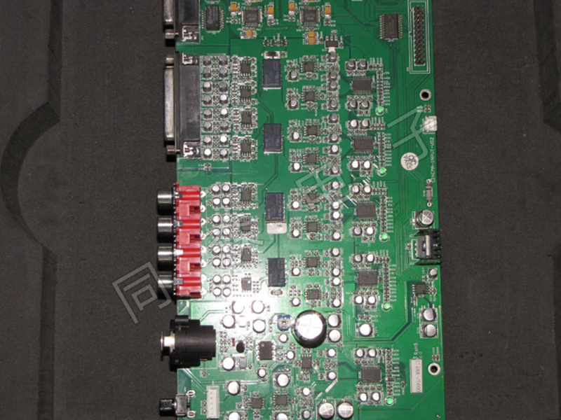
PCB location holes refer to the specific location of PCB vias determined during PCB design, which is a crucial step in the PCB design process. The function of location holes is to serve as a processing reference during printed circuit board manufacturing. There are various methods for locating PCB location holes, mainly based on different precision requirements for routing. Location holes on printed circuit boards should be represented by special graphic symbols. When the requirements are not high, larger assembly holes within the printed circuit board can also be used as a substitute.
PCB positioning holes refer to the specific location of PCB vias determined during PCB design, a crucial step in the PCB design process. Positioning holes serve as processing benchmarks during printed circuit board manufacturing. There are various methods for positioning PCB positioning holes, mainly based on different precision requirements. Positioning holes on printed circuit boards should be represented by special graphic symbols. When requirements are not high, larger assembly holes within the printed circuit board can also be used as substitutes.
To facilitate printed circuit board drilling and milling of the outer shape, to fix the board, and to facilitate online testing, many circuit board manufacturers hope that users will design three non-metallized holes on the PCB. Positioning holes are usually designed as non-metallized holes, with a drilling diameter of 3mm or 3.5mm. If the board space is tight, at least two positioning holes should be placed diagonally. If making a panel, the panel can also be considered as a PCB; the entire panel only needs three positioning holes. If the user does not place them, the circuit board manufacturer will automatically add them without affecting the circuit, or use existing non-metallized holes in the board as positioning holes.

Positioning Hole Positioning Methods
Device Holes: Most device and connector interfaces are plug-in components. The through-hole diameter of plug-in devices is 8-20mil larger than the pin diameter, ensuring good tin penetration during soldering. It should be noted that the hole diameter of the circuit board factory has an error, approximately ±0.05mm. Every 0.05mm interval represents a drill bit; for diameters above 3.20mm, every 0.1mm interval represents a drill bit. Therefore, when designing the device hole diameter, the unit should be converted to millimeters, and the hole diameter should be an integer multiple of 0.05. The board manufacturer sets the drill bit size based on the drilling data provided by the user. The drill bit size is usually 0.1-0.15mm larger than the user's required formed hole. The design hole diameter should be larger rather than smaller, and the tolerance should also be larger rather than smaller. Fewer hole diameter classifications are better. For crimped devices, the hole diameter should not be increased; it should be designed according to the recommended specifications, and it should be specified in the board manufacturing instructions which are crimped devices. This allows the circuit board manufacturer to minimize errors during board manufacturing, avoiding unnecessary trouble.
Drilling types are divided into metallized holes and non-metallized holes. Metallized holes have copper plating on the hole walls and are conductive, represented by PTH. Non-metallized holes do not have copper plating on the hole walls and are not conductive, represented by NPTH. The difference between the outer and inner diameters of the metallized hole should be greater than 20mil; otherwise, the solder ring of the pad is too small for processing and is not conducive to soldering. If conditions permit, the hole diameter can be designed as half the radius of the pad. The maximum drilling diameter for metallized holes is 6.35mm, and for non-metallized holes, it is 6.5mm. Metallized holes should not be designed on the outline; the distance between the hole edge and the outline should generally be greater than 1mm. Redrilling easily damages the drill bit, so it should be avoided as much as possible. Holes that do not require soldering and have no electrical characteristics can be designed as non-metallized holes. Non-metallized holes do not need to have pads designed; the distance between the hole edge and the line or copper foil should be at least 1mm. Drilling can be divided into circular holes and rectangular holes according to shape. Ordinary drilling is mostly circular holes. Rectangular holes are formed by drilling multiple times according to a specified procedure. Therefore, rectangular holes should be designed with a length twice the width, and the width should not be less than 0.8mm. Rectangular holes should be designed as few as possible.
PCB Positioning Hole Requirements:
The development of the PCB design industry has matured, so the requirements for PCB positioning holes are also very comprehensive. The positioning hole requirements are as follows:
1. At least two positioning holes must be set at the diagonal corners of the single board.
2. The standard diameter of the positioning hole is 3.2mm ±0.05mm.
3. For single boards of different products of the enterprise, the following preferred diameters can also be used: 2.8mm ±0.05mm, 3.0mm ±0.5mm, 3.5mm ±0.5mm, and 4.5mm ±0.5mm. For different single boards of the same product (such as the DT board and PP board of ZXJlO), if the PCB outer dimensions are the same, the positions of the positioning holes must also be unified.
4. The positioning hole is a through hole without metallization (except for RF boards).
5. If existing mounting holes (excluding handle mounting holes) meet the above requirements, no additional positioning holes need to be set.
Some Common Specifications and Precision Requirements for Positioning Holes:
1. The diameter error range of the positioning hole is generally within 0.01mm. If the error is large in the PCB manufacturing room, it will cause poor probe contact, and the automatic mechanism for aligning the interface connector will be inaccurate.
2. Diameter requirement of the positioning hole: It is best to keep it below 3mm, so that the positioning pin will not deform, and it is also inconvenient to operate if it is too large.
3. Distance between the positioning hole and the PCB network: More than 1mm, so that the installation operation is not easy to short-circuit, and will not damage the product route.
4. Type of positioning hole: Positioning holes generally need non-copper-plated mechanical holes, so that they can be separated from the circuit on the board and have higher precision.
5. Layout of positioning holes: They need to be on the four corners or diagonal lines of the PCBA, forming multi-point surface positioning, accurate positioning, and the farther the distance, the better.
6. The distance between the positioning hole and the test point should be at least 2mm to prevent accidental short circuits during testing.
7. The distance between the positioning hole and the edge of the board should be at least 2mm to ensure the strength of the PCBA and prevent cracking.
RECOMMENDED NEWS

High-end Custom Services: SMT Chip Processing Meets Diverse Industry Needs


(Telephone contact)
Email:
Address: Room 502, Building 1, No. 13, Bohua 4th Road, Huangpu District, Guangzhou City
COPYRIGHT © 2025 Guangzhou Tongsen Electronic Technology Co., Ltd. All rights reserved.