Welcome to Guangzhou Tongsen Electronic Technology Co., LTD. Website!


How to design a PCB circuit board
A PCB circuit board can combine many electronic components together, saving space and not hindering the operation of the circuit. There are many processes involved in designing a PCB circuit board. First, we need to set the various parameters of the PCB circuit board. Second, we need to place the various components in appropriate positions.
A PCB circuit board can combine many electronic components together, saving space and not hindering circuit operation. PCB circuit board design involves many processes. First, we need to set the parameters of the PCB circuit board. Second, we need to place the components in appropriate positions.
1. Enter the PCB design system and set relevant parameters
Set the design system's environmental parameters according to personal habits, such as grid size and type, cursor size and type, etc. Generally, the system's default values can be used. Parameters such as circuit board size and number of layers should also be set.
2. Generate and import the netlist
The netlist is a crucial bridge and link between circuit schematic design and printed circuit board design. Netlists can be generated from circuit schematics or extracted from existing printed circuit board files. When importing a netlist, errors in the circuit schematic design need to be checked and corrected.
3. Arrange the positions of each component package
The system's automatic placement function can be used, but this function is not perfect and requires manual adjustment of the positions of the component packages.
4. Perform circuit board routing
The prerequisite for automatic circuit board routing is to set safety distances, wire types, etc. Currently, the automatic routing function of the equipment is relatively complete, and most circuit diagrams can be routed; however, the arrangement of some lines may not be satisfactory, and manual routing can also be performed.
5. Output via printer or save a hard copy
After completing the circuit board routing, save the completed circuit diagram file, and then use various graphic output devices, such as printers or plotters, to output the circuit board routing diagram.
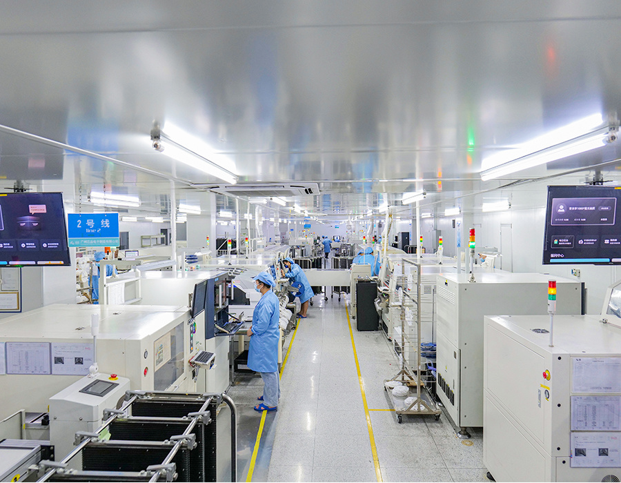
8 SMT Patching Processes
The main component of all electronic products now is the PCB board, but this PCB board also has content, generally various resistors and capacitors, etc. To firmly assemble these electronic components on the PCB board, SMT patch processing technology must be used. SMT patch processing technology provides the possibility for the miniaturization of electronic products.
Screen printing: Its function is to screen print solder paste or patch glue onto the PCB pads to prepare for component soldering. The equipment used is a screen printing machine (screen printer), located at the front end of the SMT production line. Dispensing: Drop glue onto the fixed position of the PCB board. Its main function is to fix the components to the PCB board. The equipment used is a dispensing machine, located at the front end of the SMT production line or behind the testing equipment.

Mounting: Its function is to accurately install surface mount components to the fixed positions on the PCB. The equipment used is a placement machine, located behind the screen printer in the SMT production line. Curing: Its function is to melt the patch glue, so that the surface mount components are firmly bonded to the PCB board. The equipment used is a curing oven, located behind the placement machine in the SMT production line.
Reflow soldering: Its function is to melt the solder paste, so that the surface mount components are firmly bonded to the PCB board. The equipment used is a reflow soldering oven, located behind the placement machine in the SMT production line. Cleaning: Its function is to remove harmful soldering residues such as flux from the assembled PCB board. The equipment used is a cleaning machine, the position can be fixed or not, it can be online or offline.
Inspection: Its function is to inspect the soldering quality and assembly quality of the assembled PCB board. The equipment used includes magnifying glasses, microscopes, automatic optical inspection (AOI), X-RAY inspection systems, functional testers, etc. The position can be configured in a suitable place on the production line according to the inspection needs. Rework: Its function is to rework the PCB boards that fail the inspection. The tools used include soldering irons, rework stations, etc. Configured anywhere in the production line.
RECOMMENDED NEWS

High-end Custom Services: SMT Chip Processing Meets Diverse Industry Needs


(Telephone contact)
Email:
Address: Room 502, Building 1, No. 13, Bohua 4th Road, Huangpu District, Guangzhou City
COPYRIGHT © 2025 Guangzhou Tongsen Electronic Technology Co., Ltd. All rights reserved.