Welcome to Guangzhou Tongsen Electronic Technology Co., LTD. Website!


Multilayer PCB: What it is, how it works, and when to use it
Industrial IoT: The Internet of Things revolution hinges on interconnected devices capable of processing massive amounts of data and making real-time decisions. From sensors in manufacturing plants to automated controllers, multilayer PCBs provide the necessary computing and communication capabilities in a compact design, enabling the creation of smart factories and the enhancement of industrial processes.
In the ever-evolving technological landscape of electronics, multilayer PCBs have established their dominance. Over the past few decades, multilayer printed circuit boards have become an integral part of modern electronic devices, enabling them to meet the complex demands of today's consumers.
Whether you are a newcomer to this industry awaiting the launch of new products or a seasoned electronics company, delve into this article where we will explain the intricacies of multilayer PCBs.
From Single-Sided PCBs to Double-Sided PCBs to Multilayer PCBs
Traditionally, printed circuit boards featured only one layer of conductive material. However, with the increasing number and complexity of electronic components, the demand for double-sided PCBs also increased.
These double-sided boards, featuring two conductive layers (typically a top and bottom layer), offered more space for electrical connections. Soon after, the concept of multilayer PCBs was introduced, revolutionizing the electronics industry.
What are Multilayer PCBs?
Multilayer PCBs (i.e., printed circuit boards) are an advanced type of circuit that allows for complex electronic functionalities within a compact framework.
Imagine a sandwich, but instead of bread and fillings, it's multiple layers of conductive copper separated by insulating materials. This ingenious design integrates more circuitry into a smaller space, making our devices sleeker and more powerful.
This architecture optimizes space and ensures reduced electromagnetic interference, thus enhancing performance.
Why Use Multilayer PCBs?
One of the prominent features of multilayer PCBs is their enhanced electromagnetic shielding capabilities. These PCBs effectively mitigate electromagnetic interference, ensuring signal quality, by integrating inner layers dedicated to grounding or power planes.
This meticulous layering also improves signal transmission speed, reduces crosstalk between traces, and enables unparalleled design flexibility. Designers can skillfully allocate traces, components, and power planes, customizing the design according to diverse electronic requirements.
These PCBs play a crucial role in noise reduction, thanks to their inherent design that contributes to layer-to-layer sound insulation. Furthermore, their construction facilitates a more streamlined assembly process, effectively reducing the need for interconnect harnesses.
All these factors contribute to delivering electronic products that are not only compact and lightweight but also reliable, highlighting the crucial role of multilayer PCBs in the EMS field.
Structure and Composition of Multilayer PCBs
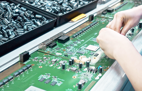
Multilayer PCB boards are constructed by stacking multiple single-layer PCBs. The foundation of these multilayer PCBs begins with the inner core board. This core board is enveloped by alternating layers of conductive copper and insulating materials. To enable electrical connections between these layers, plated-through holes are used.
The outer layers of the board primarily serve to connect electronic components, while the inner layers handle various functions such as signal transmission or power distribution.
Layer Upon Layer: The Construction of Multilayer PCBs
Multilayer doesn't just mean three or four layers; in some advanced applications, it can range from four to twelve layers, or even up to 37 layers!
The outer layers are typically covered with protective material, providing connection points for electronic components. The inner layers serve multiple functions, with some acting as ground planes to reduce electronic noise, and others as power planes for efficient power distribution.
The thickness of the copper varies depending on the specific requirements of the relevant electronic device.
Manufacturing Multilayer PCBs
The complexity of multilayer PCB manufacturing lies in ensuring that the various layers of conductive material are perfectly aligned with each other. This is achieved through a meticulous lamination process.
Sheets of copper foil and insulating layers are stacked together, and a heated hydraulic press applies high temperature and pressure to bond these layers together, achieving the desired thickness. This is followed by a precise drilling process, creating holes for electrical connections between the layers.
Advantages of Multilayer PCBs
The advantages of multilayer PCBs are multifaceted. Understanding these advantages can guide informed decisions in product development, ensuring design choices, cost-effectiveness, and the creation of devices that meet the ever-growing demands of today's technological landscape.
Advantages:
High Density: They can accommodate more components and connections in a smaller space.
Enhanced Signal Integrity: Multiple layers can shield and separate signals, preventing interference and ensuring signal transmission.
Flexible Construction Techniques: Multilayer PCBs offer designers a variety of choices regarding copper thickness, number of layers, etc.
More Powerful Capabilities: These boards have the capacity for power planes, ground planes, and multiple signal layers, accommodating the complex needs of advanced electronic devices.
Applications of Multilayer PCBs in Modern Technology
From smartphones to aerospace technology, multilayer printed circuit boards play a crucial role. As the world moves towards smaller yet robust and durable devices, the demand for multilayer PCBs is growing exponentially.
Their ability to support multiple connectors and ensure stable electrical connections makes them irreplaceable.

The applications of multilayer PCBs in several contemporary technological fields are noteworthy:
Smart Metering: As power grids become smarter and more interconnected, the need for precise data collection and real-time communication increases. Their compact design helps integrate multiple functionalities such as GSM modules, power measurement circuits, and user interfaces into a single metering device.
Telecommunications: With the rapid advancement of telecommunications, especially in the 5G and beyond era, devices require circuits that can handle high-frequency signals without interference. Multilayer PCBs, with their enhanced electromagnetic shielding capabilities, are crucial in devices such as base stations, routers, and modems. Their ability to reduce crosstalk and electromagnetic interference ensures reliable and high-speed data transmission.
Industrial IoT: The IoT revolution depends on interconnected devices capable of handling large amounts of data and making real-time decisions. From sensors in manufacturing plants to automated controllers, multilayer PCBs provide the necessary computing and communication capabilities in a compact design, enabling the creation of smart factories and the enhancement of industrial processes.
Communication Technologies: Beyond traditional telecommunications, the broader field of communication technologies—including satellite communication, maritime communication systems, etc.—is experiencing a dramatic increase in data flow.
Computers and Laptops: Motherboards in these devices commonly utilize multilayer PCBs to integrate high-speed processors, RAM, and other necessary components, ensuring efficient data processing and multitasking capabilities.
Industrial Control: Multilayer PCBs are crucial in automated equipment, CNC machine tools, and robotic systems, ensuring efficient processing and control.
In summary, any advanced electronic device or system seeking to combine complex circuitry, reliability, and space optimization could utilize the capabilities of multilayer PCBs.
RECOMMENDED NEWS

High-end Custom Services: SMT Chip Processing Meets Diverse Industry Needs


(Telephone contact)
Email:
Address: Room 502, Building 1, No. 13, Bohua 4th Road, Huangpu District, Guangzhou City
COPYRIGHT © 2025 Guangzhou Tongsen Electronic Technology Co., Ltd. All rights reserved.