Welcome to Guangzhou Tongsen Electronic Technology Co., LTD. Website!


How are PCBs manufactured? A beginner's guide to PCB manufacturing processes (Part 2)
Before a PCB reaches its destination and is integrated into an electronic device, it needs to be carefully and meticulously packaged to prevent any damage during storage and transportation. With increasingly complex supply chains, PCBs can travel across the globe before reaching their destination, so the importance of proper packaging cannot be overstated.
Steps in the Printed Circuit Board Manufacturing Process
The PCB manufacturing process begins with a blueprint and goes through complex multi-stage manufacturing phases to finally produce a functional PCB. Each step is crucial and builds upon the earlier steps of the process, which is why it is important to have a holistic understanding of the entire process when discussing how PCBs are made. In this section, we will detail each step:
Step One: Designing the PCB
The printed circuit board manufacturing process begins with the design phase, where engineers and designers use specialized software (such as Extended Gerber (IX274X)) to create blueprints outlining the layout and requirements of the PCB. PCBs come in a variety of forms, shapes, and variations, and the PCB design, layout, components, and attributes all need to perfectly match the needs of the device the PCB is intended for. This is why this process begins with a thorough research and design phase.
The software used in this phase is also crucial. They not only aid in the design but also encode essential information needed before the product goes into mass production, such as the number of copper layers, solder mask layers, and component symbols.
Step Two: Design Review and Engineering Considerations
Once the initial design is complete, the PCB undergoes a thorough review to ensure that the specifications are correct. In this phase, engineers rigorously evaluate the PCB design to look for any potential flaws, missing components, or structural issues.
Any errors not caught in this phase can lead to significant losses in subsequent phases. At a minimum, a new board design needs to be created, prototyped, and tested, and if the errors persist to the mass production phase, the entire product launch could end in failure.
After the engineers carefully review the PCB design and check for any potential errors, missing components, or structural issues, the design will be approved by the engineering team, and then we move on to the printing phase.
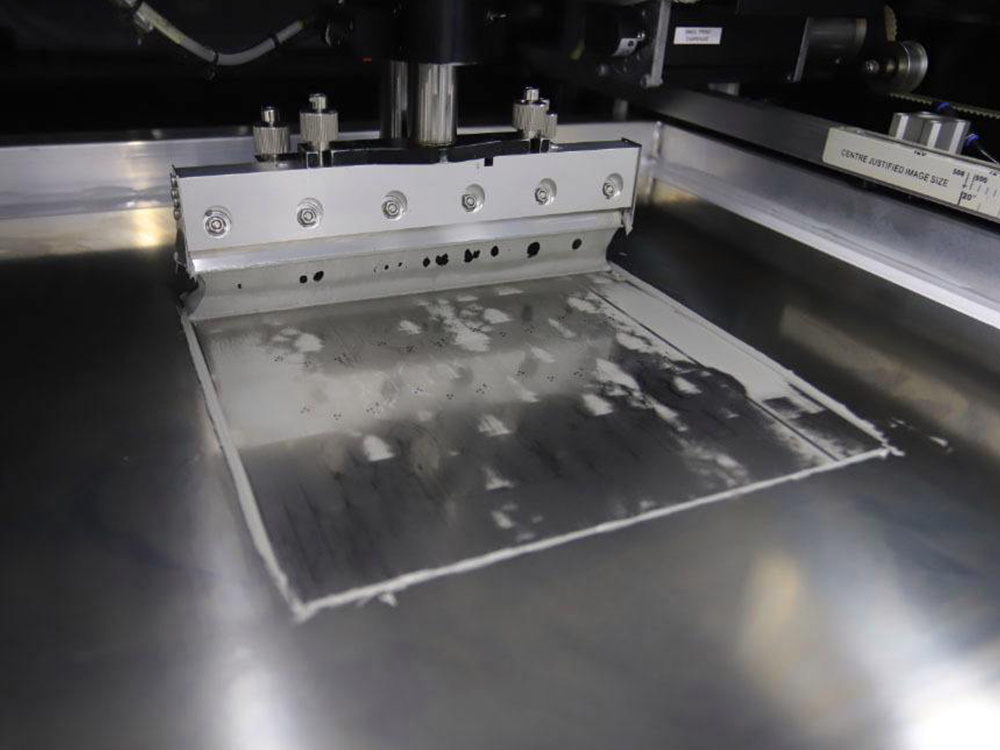
Step Three: Printing the PCB Design
The PCB design is printed using a special printer called a plotter. This printer creates a "film" of the PCB design, somewhat like a transparency. The inner layers of the PCB are represented using two colors of ink: black ink represents the copper traces, and clear ink represents the non-conductive areas. The clear ink represents the copper paths for the outer layers, while the black ink represents the areas where the copper will be removed. Registration holes are punched in the printed film to aid in alignment in subsequent steps.
While computer software and simulation technology have made significant strides and have become key parts of the circuit board design process, they alone are not enough to ensure that no mistakes are made, as the cost of errors is high. Printed circuit board design provides further opportunities to ensure the correct scaling, routing, and placement of components.
Step Four: Creating the Printed Circuit Pattern
The next phase is to create the printed circuit pattern by plating the conductive pattern with copper and then vacuuming a layer of positive photoresist material onto the surface of the foil. The printed circuit pattern mask is placed on top and exposed to ultraviolet light, making the photoresist material in the circuit design soluble. The circuit pattern mask is removed, and the circuit board is treated with an alkaline developer, exposing the exposed copper foil circuit design.
Step Five: Inner Layer Chemical Etching Process
Before proceeding, the excess and unwanted copper on the inner layers of the PCB must be removed. This is done by etching the board by exposing it to a chemical solution, which removes the exposed copper while leaving only the desired copper traces. The time and intensity of the treatment may vary depending on the design. The process of removing unwanted copper needs to be done in a strictly controlled environment to ensure that other parts of the PCB are not damaged.
The purpose of this step is to ensure that the width of the conductors perfectly matches the blueprint.
Step Six (Multi-layer PCBs only): Inner Layer Processing
In this step, the inner layers of a multi-layer PCB will undergo a series of processes. This includes imaging, etching, resist stripping, post-etch drilling, automated optical inspection, oxide application, plating, and lamination. These procedures ensure proper layer alignment, etching, and insulation of the functional multi-layer PCB.
Step Seven: Aligning the Layers
Next, we need to ensure that the layers of the PCB are perfectly aligned using the registration holes. An optical punch press helps with this operation.
There are very complex interactions between the outer and inner layers of a PCB, and slight misalignment will not only compromise the performance and durability of the board but also lead to its failure.
Step Eight: Automated Optical Inspection
Machines perform Automated Optical Inspection (AOI) to detect surface mount component (SMC) defects. The AOI compares the printed circuit board against the Extended Gerber design on multiple parameters, including circuit width and height, components, and connections.
This is a crucial step in the PCB manufacturing process to automatically identify and remove defective products from the assembly line. No matter how advanced and sophisticated the manufacturing process becomes, errors still occur frequently, but thankfully, AOI is a crucial step to ensure that these errors do not affect the final product!
Step Nine: Lamination of PCB Layers
The layers of the PCB are bonded together using epoxy-impregnated fiberglass sheets and copper foil. They are pressed together and laminated under extreme heat and pressure.
While at first glance, the lamination process may seem less important than other steps, this is a misconception. The lamination process not only improves the rigidity and integrity of the PCB but also bonds the adjacent layers and creates continuous insulation between them. Without lamination, modern PCBs would not function.
Step Ten: Drilling Process
Once the PCB layers are laminated, the drilling process begins, guided by X-rays to ensure accuracy. Using the registration holes, the excess copper is then deburred and removed.
For multi-layer PCBs, the drilling process is even more critical. When producing double-sided or multi-layer PCBs, the drilling method must ensure that the circuits on each layer are electrically connected to each other. To do this, holes are drilled and deburred in the circuit board according to a predetermined pattern, and then a layer of copper is lined inside the holes to establish conductive connections between the layers of the PCB.
Step Eleven: PCB Plating Process
After drilling, the PCB is cleaned and then chemically treated. In this process, a very thin layer of copper (only a few micrometers thick) is applied to the top layer of the board and fills the newly drilled holes. Without the plating process, these holes would expose the fiberglass substrate inside the panel.
The plating process serves multiple functions. It helps protect the outer layers of the PCB from moisture, contamination, and oxidation. They also improve the aesthetics and solderability of the PCB.
Step Twelve: Outer Layer Imaging and Etching
After imaging the outer layer with photoresist, a layer of tin is plated onto the copper as a protective layer. The etching process removes any unwanted copper and residual resist, leaving only the desired copper design.
A few millimeters of protrusion can cause problems when assembling the device the PCB is intended for. This is why this step is important to ensure that all measurements of the PCB layers and their components conform to the initial blueprint.

Step Thirteen: PCB Surface Treatment and Finishing
In this step, the PCB undergoes a series of surface treatments. First, a solder mask is applied. This is to prevent oxidation and corrosion, and also to prevent conductivity between pads.
After applying the solder mask, the PCB is cured at a high temperature in an oven. Next, important information is printed on the surface of the circuit board, such as the serial number of the circuit board, place of origin, etc. After that, surface treatment is carried out to prevent oxidation. The specific treatment on the PCB is determined by the design specifications. - Engineers will select from multiple options based on the complexity of the PCB and the expected operating environment.
Step Fourteen: Final Quality Assurance and Delivery
We have finally reached the last stage of the process. At this stage, the PCB needs to undergo various quality tests and inspections to ensure that the PCB is ready for use.
The type and number of tests the PCB needs to undergo depends on the type of PCB. For example, electrical reliability testing assesses the continuity and isolation of the circuit to ensure proper operation and design consistency.
Specific boards are neatly isolated using a profiling and routing method. Each board is cut from the panel using a CNC machine or router and shaped and sized to the required specifications. A thorough final inspection confirms hole size, dimensions, cleanliness, and overall quality.
Before the PCB reaches its destination and is integrated into an electronic device, it needs to be carefully and meticulously packaged to prevent any damage during storage and transportation. With increasingly complex supply chains, PCBs can travel around the world before reaching their destination, so the importance of proper packaging cannot be overstated.
RECOMMENDED NEWS

High-end Custom Services: SMT Chip Processing Meets Diverse Industry Needs


(Telephone contact)
Email:
Address: Room 502, Building 1, No. 13, Bohua 4th Road, Huangpu District, Guangzhou City
COPYRIGHT © 2025 Guangzhou Tongsen Electronic Technology Co., Ltd. All rights reserved.