Welcome to Guangzhou Tongsen Electronic Technology Co., LTD. Website!


What is the PCB manufacturing process?
Once the PCB manufacturing process is complete, the finished circuit boards undergo a series of inspections and tests before assembly or shipment to ensure their functionality. Automated testing equipment checks for any short circuits that may affect the board's function; any PCBs that fail the test are discarded.
PCB manufacturing is the process of creating a bare board, which will serve as the foundation for printed circuit board assembly.
You should carefully select your PCB manufacturing contractor, as even small errors can ruin the entire board, leading to product scrap. Communication between the design team and the manufacturer is critical, especially as manufacturing has moved overseas.
What is the difference between the PCB manufacturing and PCB assembly process?
PCB manufacturing and PCB assembly are two distinct parts of the PCB manufacturing process.
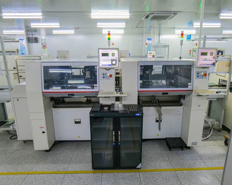
PCB manufacturing is the process of transcribing the circuit board design onto the physical structure of the board. In contrast, PCB assembly is the process of actually placing components onto the board to make it functional. PCB manufacturing can be likened to the roads, streets, and zoning of a city, while PCB assembly is the actual buildings that allow the printed circuit board to function. For more information on PCB assembly, click here.
Steps Before Beginning the PCB Manufacturing Process
The key to manufacturing a printed circuit board lies in the details. The initial design must be finalized, as even one unsynchronized component update can lead to a poorly constructed board. This includes:
A complete circuit engineering review;
Synchronized schematic and layout databases;
Completed circuit simulation, signal integrity, and power integrity analysis;
Checking PCB design rules and constraints;
Reviewing the bill of materials and manufacturing design rules;
PCB Manufacturing Process
Laser Direct Imaging and Develop/Etch/Strip Process
Before beginning PCB manufacturing, laser direct imaging (LDI) is used to apply the areas that will become the traces, pads, and metal grounds of the printed circuit board.
A dry film is applied to the copper clad board.
Laser direct imaging exposes certain parts of the board to light in the shape of the PCB pattern.
Any unexposed portions of the board are developed away, leaving the remaining film as an etch resist
The remaining film acts as an etch resist, removing it from the exposed copper to form the copper circuitry.
Afterward, automated optical inspection checks for defects before the layers are pressed together. Any errors, such as potential shorts or opens, can be corrected at this stage.
Oxidation and Lamination
After all layers are etched, the inner layers of the printed circuit board undergo a chemical treatment called oxidation to improve adhesion strength. Then, alternating layers of prepreg and copper foil are laminated together using heat and a hydraulic press. Prepreg is a fiberglass material containing epoxy resin, which melts under the heat and pressure of lamination, bonding the layers together into a "PCB sandwich".
Special care must be taken to ensure that the circuitry on each layer remains aligned.
Drilling
In order for multilayer printed circuit boards to send signals from one layer to another, holes must be drilled or laser-ablated to create vias that connect the layers. The drilling method varies depending on the type of via used, but it is typically done on 2-3 panels at once. The final result is usually 5 mils larger than the product because these holes will be plated with copper to help send electrical signals through a process called electroless copper plating.
Blind and buried vias need to be made before the lamination process. Incorporating these into the PCB design can add cost because extra steps must be taken.
Electroless Copper Plating and Outer Layer Dry Film
After the surface is drilled, chemical and mechanical processes are used to clean away excess resin and debris. After cleaning, a thin layer of copper is deposited on all exposed portions of the panel, providing a metallic base for the plating process. Similar to the previous develop/etch/strip process, a dry film is applied to the outer layers of the copper board, and then laser direct imaging is performed, leaving behind the conductive pattern.
Plating, Stripping, and Etching
The conductive patterns and drilled holes are exposed, and then the panel is placed in a plating bath containing sulfuric acid and copper sulfate. When a current is passed through it, copper is deposited on the conductive surfaces of the board, approximately 1 mil thick. The board is then removed and placed in a tin plating bath, which acts as an etch resist.
After plating, the dry film is removed, and the exposed copper not covered by tin is etched away, leaving only the traces, pads, and other patterns on the board. The remaining tin is then chemically stripped away, leaving only copper in the precise areas.
At this point, the printed circuit board is assembled—but not quite ready for assembly.
Solder Mask, Silkscreen, and Surface Finish
Before entering the PCB assembly phase, the printed circuit board will have a solder mask applied using a similar UV exposure process as the photoresist stage. This gives the printed circuit board its distinctive green color, although other options are available.
The solder mask is a thin layer of polymer that prevents the copper traces printed on the board from oxidizing. It also prevents solder bridges—when an unintended connection forms between two conductors, affecting the functionality of the printed circuit board.
The solder mask color is optional at this stage, but manufacturers typically use green because its high contrast and trace visibility, crucial for the PCB prototyping phase, aids in defect inspection. Solder mask color typically does not affect the functionality of the board, but darker colors absorb more heat and are therefore unsuitable for high-temperature applications.
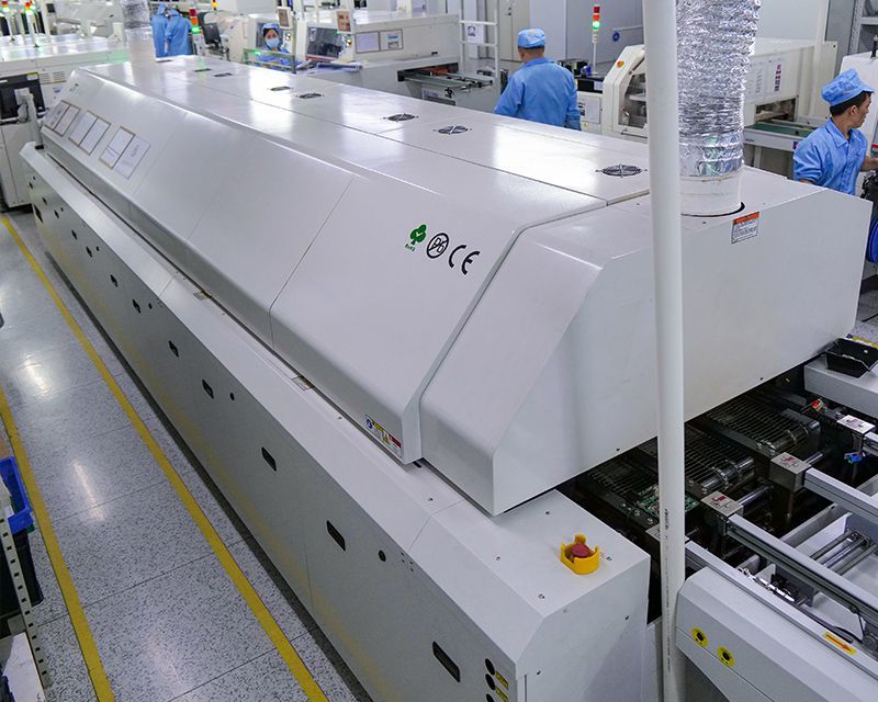
After the solder mask is applied, component reference markings and additional board markings are silkscreened onto the printed circuit board. The board is then baked in an oven to cure the solder mask and silkscreen ink.
The exposed metal surfaces not covered by the solder mask are given a surface finish. This protects the metal and aids in the soldering process during PCB assembly.
Assembly Preparation, Inspection, and Testing
Once the PCB manufacturing process is complete, the finished circuit boards undergo a series of inspections and tests before assembly or shipment to ensure their proper functionality. Automated testing equipment checks for any short circuits that could affect the board's function; any PCBs that fail the tests are discarded.
Previous
RECOMMENDED NEWS

High-end Custom Services: SMT Chip Processing Meets Diverse Industry Needs


(Telephone contact)
Email:
Address: Room 502, Building 1, No. 13, Bohua 4th Road, Huangpu District, Guangzhou City
COPYRIGHT © 2025 Guangzhou Tongsen Electronic Technology Co., Ltd. All rights reserved.