Welcome to Guangzhou Tongsen Electronic Technology Co., LTD. Website!


5 Key Stages in PCB Manufacturing
This is a step in PCB manufacturing, mainly involving positioning various electronic components onto their respective holes. This can be achieved through through-hole technology or surface mount technology. A commonality between these two technologies is that the component leads are electrically and mechanically secured to the circuit board using molten metal solder.
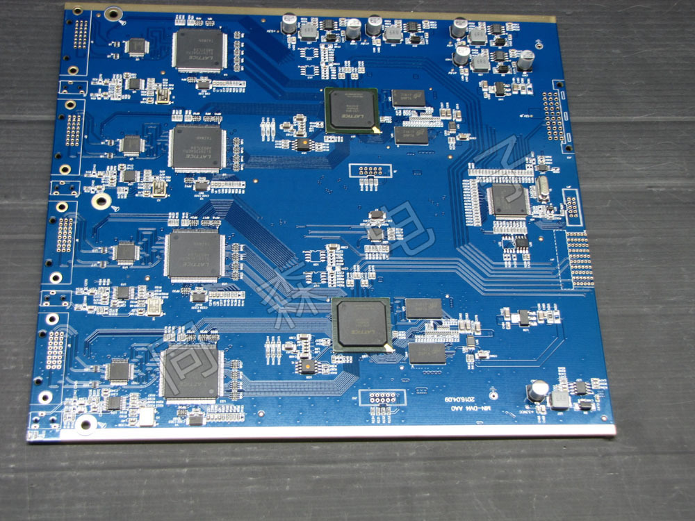
Printed Circuit Boards (PCBs) are one of the indispensable elements in almost all electronic applications. They bring life and function to electronic and electromechanical devices by routing signals within the circuit. Many people know what PCBs are, but only a few know how they are manufactured. Today, PCBs are constructed using a patterned electroplating process. They proceed to the next stage, mainly including etching and stripping. This article will effectively guide you through the various stages of the printed circuit board design process, but will focus more on the etching and stripping process of the board.
PCB Design and Manufacturing Process
Depending on the manufacturer, the PCB manufacturing process may vary slightly, especially in component mounting techniques, testing methods, etc. They use various automated machines for mass production, including drilling, plating, punching, etc. Apart from some minor differences, the main stages involved in the PCB manufacturing process are the same.
Stage 1: 8-Step Guide to Etching PCBs
PCBs are made by bonding a layer of copper across the entire substrate. Sometimes, both sides of the substrate are covered with a copper layer. The PCB etching process, also known as the controlled level process, uses a temporary mask to remove excess copper from the PCB panel. After the etching process is complete, the desired copper traces remain on the circuit board. The PCB etching process uses a highly corrosive amine solution - ferric chloride or hydrochloric acid. Both of these chemicals are considered economical and abundant. To etch a PCB, you need to follow these steps.
Step 1:
Circuit board design is the initial stage of the etching process, and can be done using any software of your choice. Once the design is complete, print it on transfer paper. Make sure the design is suitable for the glossy side of the paper.
Step 2:
Now, neatly polish the copper plate so that its surface is rough enough to accommodate the circuit board design. The following points need to be remembered when performing this step:
When handling etching solutions, wear surgical gloves or safety gloves. This will prevent oil from transferring to the copper plate and your hands.
When polishing the copper plate, make sure to cover all edges of the copper plate.
Step 3: Clean the copper plate with water and rubbing alcohol. This will remove fine copper particles from the surface of the plate. After cleaning, allow the plate to dry completely.
Step 4: Accurately cut out the PCB design diagram and place the circuit board face down on the copper plate. Now, the circuit board needs to be laminated multiple times until the heating is complete.
Step 5: Once the plate is heated, remove it from the laminator and place it in a cold water bath. Agitate the plate for a while to allow the paper to float to the surface.
Step 6: Remove the circuit design from the slot and place it in the etching solution. Agitate the plate again for half an hour, this will help dissolve the unwanted copper around the design.
Step 7: After washing away the excess copper in a water bath, allow the plate to dry. Once the copper plate is completely dry, wipe off the ink transferred to the circuit board design with alcohol.
Step 8: Now you are ready to etch the circuit board; however, you will need to use the appropriate tools to drill holes.
Stage Two: PCB Stripping Process
Even after the etching process, a certain amount of copper remains on the circuit board, which will be covered with tin/lead or electroplated tin. Nitric acid effectively removes tin while keeping the copper circuit cracks under the tin metal. Therefore, you will obtain a clear copper outline on the circuit board, and the circuit board is ready for the next process - solder resist.
Stage Three: Solder Resist
This is an important process in the PCN design process, using solder resist material to cover the unsoldered areas on the circuit board. This prevents solder from forming traces, thus avoiding the formation of shortcuts to the leads of adjacent components.
Stage Four: PCB Testing
After the PCB is manufactured, testing is crucial to check its functionality and characteristics. In this way, PCB manufacturers can determine whether the circuit board is working as expected. Today, PCB testing uses a variety of advanced testing equipment. ATG testers are mainly used to test large batches of PCBs, including flying probe testers and fixtureless testers.
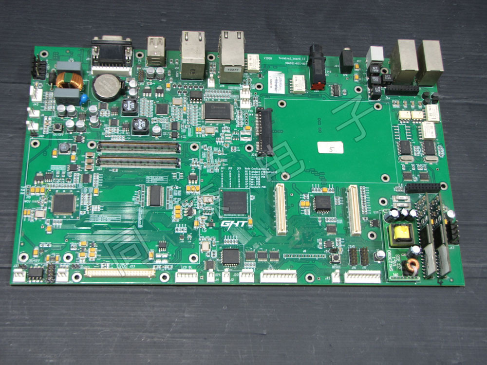
Stage Five: PCB Assembly
This is a step in PCB manufacturing, mainly involving positioning various electronic components onto their respective holes. This can be achieved through through-hole technology or surface mount technology. A commonality between these two technologies is that the leads of the components are electrically and mechanically secured to the circuit board using molten metal solder.
RECOMMENDED NEWS

High-end Custom Services: SMT Chip Processing Meets Diverse Industry Needs


(Telephone contact)
Email:
Address: Room 502, Building 1, No. 13, Bohua 4th Road, Huangpu District, Guangzhou City
COPYRIGHT © 2025 Guangzhou Tongsen Electronic Technology Co., Ltd. All rights reserved.