Welcome to Guangzhou Tongsen Electronic Technology Co., LTD. Website!


Automated PCB manufacturing process in smart factories
Meanwhile, printed circuit boards have been widely used for decades, and the manufacturing process has therefore matured. Year after year of incremental improvements often yields incredible results. Consider this the next time you order a large quantity of high-quality PCBs at a low price for fast delivery.
Whether you're a professional electronics designer or a hobbyist, you can receive high-quality custom printed circuit boards (PCBs) within a week of ordering, and in some cases even faster. The price of these PCBs is so low, you might question how they're manufactured. The answer is largely due to the highly automated smart factory concept used in production, starting from the ordering process itself.
After designing your board using Electronic Design Automation (EDA) software (such as KiCad, Eagle, or Altium), the PCB fabrication facility (often shortened to "factory") proceeds with the automated PCB manufacturing process. You (virtually) draw a set of standard instructions (typically Gerber files in RS-274X or RS-274X2 format) along with drill files. These are then uploaded to your chosen PCB manufacturer. Many vendors (such as OSHPark and PCBWay) will provide you with an instant quote, and you can order your boards based on the quote.
The manufacturer typically checks the uploaded board to ensure that design rules haven't been violated, so that the PCB is correctly made. This involves a significant amount of automation, but may require some human intervention and/or back-and-forth communication. After checking and communication, multiple customer boards are combined onto a single panel awaiting cutting. Typically, these panels are cut to standard sizes for the factory process, with outer layers of copper and inner layers of FR4 (fiberglass) substrate to provide strength and insulation.
Elements of the Automated PCB Manufacturing Process
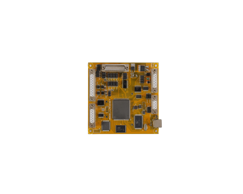
While it's impossible to describe here the complexities of how all PCB manufacturers do things, we can break down the automated PCB manufacturing process into several key elements. Note that for simplicity, we will consider double-sided board manufacturing, but more layers can be used via stacking and bonding processes as needed. Furthermore, while this smart manufacturing process involves a high degree of automation, human intervention is still required for tasks such as transporting work-in-progress, machine setup, and final inspection.
1. Drilling Through-Holes and Vias
Typically, one step in the PCB manufacturing process (after cleaning and deburring operations) is drilling through-hole components and vias. This operation is done on a drilling machine capable of forming holes as small as 100 microns, smaller than a human hair (approximately 150 microns in diameter). The changing of drill bits of different diameters is automated.
2. Photolithography and Layer Etching
To form the PCB traces and copper fill areas, a negative image of the finished copper is printed onto a transparent sheet according to the provided Gerber information. Both sides of the panel are coated with a photosensitive film called photoresist. The printed sheet is aligned with the top and bottom of the panel, and then a UV lamp is used to harden the photoresist in areas of the film where there is no printed image. Further processing washes away the unhardened photoresist along with the underlying copper.
At this point, the circuit board is still part of the entire panel, which may contain many designs. Throughout the PCB manufacturing operation, cleaning is done at many points, and various checks (including optical processes) are progressively performed to catch errors early.
3. Plating and Chemical Processes
Additional copper is plated onto the PCB to create conductive pathways for via and through-hole connections, and to build up the original foil. Different thicknesses of copper plating can be specified, and the entire process is tightly controlled to meet customer requirements.
4. Solder Mask, Silkscreen, Hot Air
A solder mask is used to protect the copper traces and is applied in liquid form to both sides of the PCB. After application, the board is baked to a semi-hardened state, and then a transparent printed sheet is applied to both sides. A UV process hardens the exposed solder mask, and then the unexposed solder mask is removed, similar to the photoresist process performed earlier.
A visible silkscreen layer is then printed using an inkjet printer for component identification and other marking purposes. Processes such as Hot Air Solder Leveling (HASL) are typically performed to protect exposed pads from oxidation. A flying probe test can then be performed to ensure that the PCB conducts and resists current as designed.
5. Profiling and Routing
After each PCB on the panel has been properly processed and inspected, a computer-controlled routing operation cuts the outline of the circuit board and internal features that are not through-holes. These edges and features do not have to be straight. Before this process, the panel can also undergo V-scoring (partially cutting into a "V" shape). V-scoring is limited to straight lines and allows the customer to break apart the modules upon receipt.
6. Finishing, Packaging, Shipping
After final cleaning, further processing to remove artifacts from routing, and inspection, the PCBs are ready to be packaged and shipped to the customer. It's a remarkable process.
PCBs: Process and Fulfillment Optimization
While impressive, note that the process outlined here is a simplification, and these operations vary by manufacturer and even product. Beyond automation, consider geographical arbitrage, geopolitics, shipping, and many other factors for a complete picture of how fast-turnaround PCBs are produced at affordable prices.
Meanwhile, printed circuit boards have been in widespread use for decades, and the manufacturing process has matured accordingly. Incremental improvements year after year tend to have incredible effects. Consider this the next time you order a large quantity of high-quality PCBs at a low price for fast delivery.
RECOMMENDED NEWS

High-end Custom Services: SMT Chip Processing Meets Diverse Industry Needs


(Telephone contact)
Email:
Address: Room 502, Building 1, No. 13, Bohua 4th Road, Huangpu District, Guangzhou City
COPYRIGHT © 2025 Guangzhou Tongsen Electronic Technology Co., Ltd. All rights reserved.