Welcome to Guangzhou Tongsen Electronic Technology Co., LTD. Website!


SMT Stencil Introduction and Basic Knowledge (Guangzhou Tongsen Electronic Training Content)
SMT Stencil Introduction and Basic Knowledge (Guangzhou Tongsen Electronic Training Content)
Tongsen Electronic SMT Surface Mount Technology Stencil Introduction
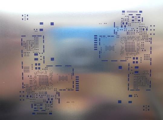
SMT surface mount technology determines the product's yield rate and appearance. Stencils are made using laser cutting or etching, with etching gradually being phased out;
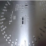
Stencil sizes include 37*47, 42*52, 55*65, 60*65cm, 65*65cm, and 73.6*73.6cm. Our automatic printing machines use 55*65cm stencils, with a minimum of 42*52cm. Stencils are categorized into solder paste stencils, red glue stencils, and dual-process stencils (copper stencils), as well as stepped stencils. Stencil sheet thicknesses range from 0.8MM, 1.0MM, 1.2MM, 0.13MM, 0.15MM, 0.18MM, 0.2MM, 0.25MM, to 0.3MM. Thicknesses of 0.05mm—0.15mm are generally required for solder paste stencils, while 0.18mm—0.3mm are generally required for red glue stencils.
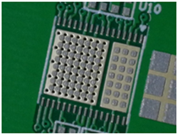
1. Solder Paste Stencils:
Thicker stencils deposit more solder, easily leading to solder bridging and short circuits. Currently, 1.0MM is more common; for customers requiring more solder on the pads, the solder pads of CHIP components can be enlarged; however, thick sheets should be avoided to prevent short circuits in ICs or densely-packed components.
For special pads prone to short circuits, the corresponding stencil openings can be reduced, or a thinner stencil can be selected. Reducing stencil openings or using anti-bridging stencils can prevent solder bridging.
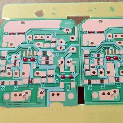
2. Red Glue Stencils:
During production, blocked holes are a major concern. The boards produced require frequent push force testing. This process is gradually being phased out due to the high defect rate associated with the evolution of high-power components and smaller CHIP components. Currently, it is only used for power boards. The most common problems with this production process are component collisions and glue overflow.
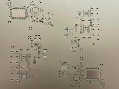
3. SMT Stepped Stencils
These are designed to accommodate the varying solder volume requirements of different sized components on the same PCB.
They can be categorized into: locally thickened stencils (i.e., large-area thinning) and locally thinned stencils (small-area thinning).
Locally thickened stencils are generally suitable for larger components, such as IC grounding, sockets, and modules that require a large amount of solder.
Locally thinned stencils are generally suitable for more precise components, such as precision ICs and 0.4-0.5 pitch BGAs that require slightly less solder.
4. Dual-Process Copper Stencils:
When a single PCB side requires both solder paste and red glue application, dual-process stencils are used.
RECOMMENDED NEWS

High-end Custom Services: SMT Chip Processing Meets Diverse Industry Needs


(Telephone contact)
Email:
Address: Room 502, Building 1, No. 13, Bohua 4th Road, Huangpu District, Guangzhou City
COPYRIGHT © 2025 Guangzhou Tongsen Electronic Technology Co., Ltd. All rights reserved.