Welcome to Guangzhou Tongsen Electronic Technology Co., LTD. Website!


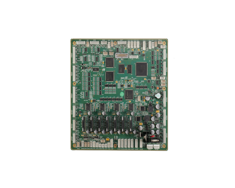
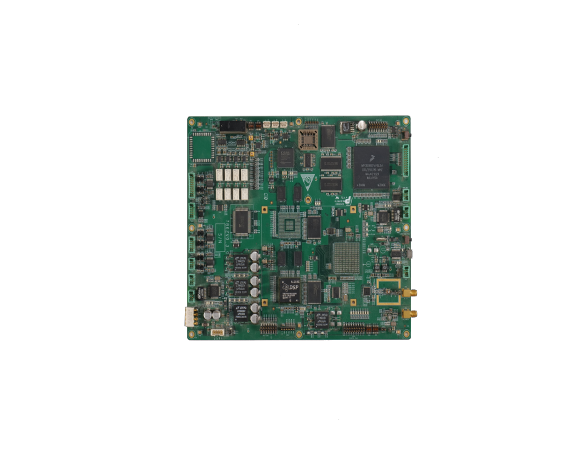
PCB Manufacturing Process: A Comprehensive Guide (Part 2)
This stage involves packaging and shipping the PCB to its intended destination. Standard packaging is designed to protect the PCB from dust and other environmental factors. However, packaging may vary according to customer specifications.
3. Ultraviolet Sandblasting
The resist consists of a layer of photoreactive chemicals. We expose the resist-coated laminate to ultraviolet or UV light, hardening the layer of photoreactive chemicals.
● Ultraviolet light passes through the translucent portions of the film, hardening the photoresist
● However, ultraviolet light cannot harden the areas of black ink
● Only the hardened areas are retained as copper pathways; the rest of the circuit board is discarded
● The circuit board is cleaned with an alkaline solution to remove photoresist residue
● Finally, high-pressure water is used to remove any remaining residue
● The circuit board is dried
● Technicians check the circuit board for errors before proceeding to the next step
The purpose of using photoresist and ultraviolet sandblasting is to ensure that the actual PCB manufacturing perfectly matches the schematic blueprint.
4. Etching the Inner Layers
Cleanliness of the circuitry is important in PCB manufacturing. Therefore, this PCB manufacturing process removes excess copper from the board. Otherwise, a single speck of dust could cause a short circuit or an open circuit. After this step, you will only have the copper needed to manufacture the PCB.
● Typically, the inner layer copper will be removed via chemical etching
● The photoresist protects the necessary copper on the circuit board from etching
● The time and solvent required for etching may vary depending on the size of the circuit board
● Larger circuit boards typically require more time and/or solvent
5. Layer Alignment
After cleaning, the laminate is ready for layer alignment. Generally, we use an optical punch, a specialized machine that uses needles through alignment holes to align the inner and outer layers.
6. Optical Inspection
Once the layers are cleaned and ready, they need to be correctly aligned. Therefore, technicians place the layers into an optical punch.
This is known as optical inspection. It ensures that the PCB is free of defects, as there is no room for error correction once the layers are combined.
● Designers will use an Automated Optical Inspection (AOI) machine for inspection.
● The AOI machine compares the PCB to the original schematic.
● The AOI machine uses laser sensors to scan the layers and perform an electronic comparison
● We discard defective circuit boards at this stage.
● The process is repeated after imaging and etching the outer layers.
7. Laminating and Pressing the Layers
At this stage of printed circuit board manufacturing, the PCB begins to take shape. The defect-free layers are fused and bonded together to form the PCB through the following two steps.
Stacking or Layering
This process sandwiches the PCB outer layers (made of pre-preg epoxy fiberglass) and thin copper foil layers (with etching for copper lines) in between. This process is done using metal fixtures on a specialized lamination press.
● The operator uses specialized pins to mount each layer onto the worktable
● First, the operator places a layer of pre-preg epoxy (called prepreg) on the alignment tray of the worktable
● Next, they place a layer of substrate on the prepreg epoxy
● A layer of copper foil is placed on the substrate layer ●
More prepreg resin sheets are placed on the copper foil layer
● The stack is completed with a copper or aluminum platen
● The operator ensures that the stack is perfectly aligned to prevent shifting during alignment
● Now, the stack is ready for bonding
Lamination or Bonding
Before bonding, the operator places the stack on a mechanical press to fuse the layers together.
● The operator places the stack on the laminator
● The laminator is computer-controlled
● The computer will heat the press plates and apply pressure according to calibration, fusing the PCB layers
● After removing the top platen and pins, the technician pulls out the printed circuit board.
8. Drilling
Drilling is considered a crucial step in the PCB manufacturing process, laying the foundation for vias and connections between different PCB layers.
All planned subsequent components, such as copper connecting vias and leads, rely on the accuracy of precise drilling.
PCB drilling requires high precision, as even minor errors can result in considerable economic losses.
This is why leading professional Chinese PCB manufacturers tend to use computer-controlled PCB drilling machines. These machines can drill holes as small as 100 micrometers in diameter using pneumatic spindles rotating at 150,000 RPM. Drilling also takes time, as the average PCB has over one hundred drill points.
● Before drilling, an X-ray locator is used to determine the location of the drill points
● A backing material board is placed under the drilling target to ensure a clean drill
● First, alignment holes or guide holes are drilled to secure the PCB stack
● The computer-controlled machine uses the original design as a guide to drill the target
After drilling, remove the extra copper layer around the edges using contouring.
9. PCB Plating
After drilling, the next step is plating. PCB plating is the process of filling the drilled holes with copper to allow current to flow from the surface of the board to the inner layers, between two layers, or between two surfaces. This process involves a series of chemical baths.
Thoroughly clean the PCB panel.
Place the panel in a series of chemical baths to deposit a thin layer of copper approximately 1 micron thick.
Use a computer to control the PCB plating process.
10. Outer Layer Imaging
Similar to step two, this step also involves applying another photoresist to the PCB panel. However, the photoresist is only applied to the outer layer for imaging. This process takes place in a sterile environment.
Secure the black ink transparency film with pins to prevent misalignment.
The PCB panel, after being coated with photoresist, enters the yellow room.
UV irradiation hardens the photoresist.
Remove the uncured photoresist protected by the black ink.
11. Outer Layer Etching
Outer layer etching prepares the PCB panel for AOI (Automated Optical Inspection) and soldering. During this process, the unnecessary copper on the outer layer is removed.
Apply a layer of copper using electroplating.
After the initial copper bath, use tin plating to protect the copper in key areas.
The PCB board undergoes Automated Optical Inspection (AOI) to ensure the copper layer meets the required specifications.
12. Solder Mask Application
This application is necessary as it adds a protective layer to the outer surface of the printed circuit board, preparing it for the soldering process. It essentially masks the areas that don't need soldering.
Clean the PCB board, removing impurities or excess copper.
Apply a layer of epoxy ink and solder mask to the surface.
Use UV sandblasting to indicate areas that do not require soldering.
Remove from the unnecessary areas.
Place the circuit board in an oven to cure the solder.
13. Screen Printing
Screen printing is the process of using an inkjet printer to print all the information directly onto the circuit board. It typically includes:
Company ID
Warning labels
Logos or symbols
Component numbers
Pin locators and other markings
14. Surface Finishing
The near-finished PCB board needs to be coated with a conductive material, generally according to customer specifications. This adds extra solderability to the PCB. This process allows for surface smoothness.
15. Testing
PCB testing is also a crucial step in the manufacturing process. We will use different testing methods to ensure the PCB functions correctly and meets the original design specifications. We will detail the established PCB testing methods in a later article.
16. Profiling
Profiling is essentially a post-step in the PCB manufacturing process. Before this, the printed circuit board is a single constructed panel. Using the original design file, the PCB is cut into individual boards. There are two common methods for separating PCB boards:
Scoring: Also known as routing, this method involves cutting several small notches along the edges of the board.
V-Grooving: In this method, a CNC machine makes a V-shaped cut along the side of the PCB board.
Regardless of the method used, after profiling, you can easily break the PCB board.
17. Final Quality Check
After profiling, each printed circuit board undergoes a final visual inspection and quality check. The manufacturer will package and ship the error-free PCBs after the final inspection.
The following checks help identify error-free and functional PCBs:
Repair and retest all boards that fail the PCB inspection.
Make all PCBs perfectly match their original design specifications.
Inspect and maintain a sterile environment to prevent contamination and errors.
Check all finished PCBs for burrs or sharp edges.
Make the hole sizes of all layers perfectly match.
Make the hole sizes meet the design specifications.
18. Packaging and Shipping
This stage involves packaging and shipping the PCBs to their intended destination. Standard packaging designs protect the PCBs from dust and other environmental factors. However, packaging may change according to customer specifications.
Previous :
RECOMMENDED NEWS

High-end Custom Services: SMT Chip Processing Meets Diverse Industry Needs


(Telephone contact)
Email:
Address: Room 502, Building 1, No. 13, Bohua 4th Road, Huangpu District, Guangzhou City
COPYRIGHT © 2025 Guangzhou Tongsen Electronic Technology Co., Ltd. All rights reserved.