Welcome to Guangzhou Tongsen Electronic Technology Co., LTD. Website!


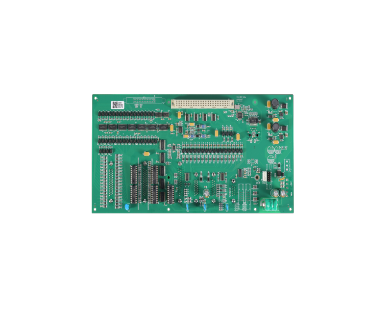
Rigid PCB manufacturing
After completing all the above steps, the PCB will be sent for testing before assembly. Depending on the design requirements and complexity (e.g., HDI design, flexible PCB design, metal core design, etc.), other steps and processes may be involved in the PCB manufacturing process.
PCB manufacturing is a multi-step process, starting from product conception and culminating in an assemblable PCB. The standard PCB manufacturing process is one of two steps in PCBA manufacturing, where the circuit board's design data is translated into a physical structure according to the provided design specifications. The steps involved in the manufacturing process depend on the complexity of the PCB; it is important not to skip any steps to achieve the performance of the final product.
All printed circuit boards are manufactured based on certain substrates, with epoxy-filled fiberglass substrates being commonly used. However, some applications require flexible PCBs, and therefore their substrates are made of easily bendable materials such as polyimide or Kapton plastic. Other applications (such as RF PCBs) will require PTFE substrates to support low-loss signal propagation, or high-power systems may require metal-substrate PCBs.
Circuit Image Transfer Methods
The PCB manufacturing process begins with transferring the design data from the design file to the printed circuit board. The purpose of this step is to etch away the copper on the substrate, leaving behind the conductive copper elements that make up the PCB circuitry. The printing process can be broadly classified into two categories:
Traditional Photo Imaging Tools
Laser Direct Imaging (LDI)
Photolithography is a traditional method of transferring the circuit design from a file to a film (template). A special printer called a photoplotter is used to create the film, which is then used to transfer the copper circuit to the circuit board. Photoplotter technology provides high-definition film of printed circuit components through precise printing. The photolithographic negative image is printed on a transparent plastic sheet with black ink, which will serve as a mask for exposing the photoresist material coated on the copper.
Generally, the transparent parts of the sheet represent the non-conductive parts of the PCB, while the black ink printed patterns represent the conductive copper areas. This is the standard followed for the inner layers of the PCB. The printing of the outer layer film follows the opposite convention: the black parts refer to the parts that will be etched away, while the transparent parts represent the copper areas.
For LDI, a precisely focused, computer-controlled scanning laser beam can be used to transfer the circuit pattern directly onto the PCB. This technology is very precise, and there are no alignment issues that are typically associated with photoplotter tool methods. In addition, since films degrade over time, they usually need to be replaced periodically. Laser direct imaging does not have this problem because it does not require a medium to transfer the image to the PCB.
Inner Layer Printing and Etching
The pre-bonded copper laminate is coated with a photoresist material, and this photoresist layer is exposed to ultraviolet light by printing a layer film. In the case of direct imaging technology, a laser beam is used instead of ultraviolet light. This optical exposure results in the photoresist material hardening into a pattern that matches the copper circuit. The remaining areas remain flexible and can be easily removed with chemicals. The unwanted copper portions are removed from the board through an etching process, leaving behind the printed circuit pattern blocked by the hardened photoresist. Finally, the PCB is chemically cleaned to remove the photoresist, and then the circuit board is transferred to the next stage.
Multilayer PCBs are made by stacking multiple layers. After all layers are cleaned and prepared, alignment punches are used to ensure that there is no misalignment between the layers. Alignment holes are used to align the inner layers with the outer layers. A machine called an "optical punch" is commonly used for this purpose.
The next step is to ensure that the inner layer circuit boards are manufactured as expected by the design database, so the PCB enters the inspection stage. Automated optical inspection is a popular PCB inspection method because it can be used to identify manufacturing defects. This method involves using a computer to automatically check the inner layers for incomplete designs or remaining resist material. Once the PCB passes inspection, it proceeds to the next stage.
PCB Layer Stack Lamination
A press is used to align, heat, and bond the layers, placing copper foil and insulating material between them. The insulating material is usually glass fiber pre-impregnated with epoxy resin, also known as "prepreg". The heat and pressure generated by the lamination process melt the resin in the prepreg, and as the resin cools, the prepreg will fuse with the other layers in the PCB stack. If your circuit board is sent to a manufacturing workshop, the manufacturer usually uses copper-clad laminates provided by material suppliers.
PCB Drilling and Plating
After printing, etching, cleaning, and laminating the PCB, the next step is drilling to mount the components. For multilayer printed circuit boards, through-holes must be drilled or laser-cut to connect the layers in order to transfer signals from one layer to the next. Numerical drilling data prepared according to the PCB design data is used to indicate the drilling locations, and an X-ray machine is used to precisely locate the drilling points. Before drilling, the PCB layers are fixed using guide holes or tooling holes on the PCB panel.
After drilling and removing debris, the next step in the PCB manufacturing process is to plate the outer layers with copper. This involves exposing the PCB to various electrolyte solutions, during which copper will establish connections along the through-holes and exposed copper.
Layer Imaging
Outer layer imaging uses the same technology as the inner layers. First, a photoresist material is applied to the outer layer, and then the photoresist is exposed to ultraviolet light using an optical image transfer method. Ultraviolet light exposure hardens the photoresist material, but unnecessary parts of the PCB will harden, while the photoresist on the circuit remains flexible. The unexposed photoresist is then washed away, and the circuit board is plated with copper. As a final step, the outer layer is also tin-plated to protect the copper underneath. Finally, the outer layer undergoes a final etching process to remove any unwanted residual copper. The outer layer is also inspected via automated optical inspection.
Solder Mask and Silkscreen Application
A solder mask is a polymer layer that protects the copper from high-temperature solder, conductors that may cause short circuits on the circuit board, environmental exposure, and any substances that may cause mechanical damage to the outer layers. The solder mask material is placed using ultraviolet light exposure. In addition to the solder mask, component reference designations and other markings are silkscreened onto the circuit board.
After all the above steps are completed, the PCB will be sent for testing before the assembly process. Depending on the design requirements and complexity (e.g., HDI designs, flexible PCB designs, metal core designs, etc.), other steps and processes may also be involved in the PCB manufacturing process.
Previous
RECOMMENDED NEWS

High-end Custom Services: SMT Chip Processing Meets Diverse Industry Needs


(Telephone contact)
Email:
Address: Room 502, Building 1, No. 13, Bohua 4th Road, Huangpu District, Guangzhou City
COPYRIGHT © 2025 Guangzhou Tongsen Electronic Technology Co., Ltd. All rights reserved.