Welcome to Guangzhou Tongsen Electronic Technology Co., LTD. Website!


PCB Manufacturing Process: A Comprehensive Guide
This step in the PCB manufacturing process marks the beginning of the actual PCB manufacturing. The process starts with the basic shape of the PCB, which includes a laminate made of substrate material. The substrate material is typically epoxy resin and fiberglass.
What is a PCB?
PCB stands for Printed Circuit Board. It mechanically supports and electrically connects various components in a circuit.
A basic printed circuit board design consists of a flat piece of insulating material and a layer of copper foil laminated onto a non-conductive substrate (usually fiberglass).
PCB circuit boards use conductive pathways, tracks, or signal lines etched from a copper sheet to connect the board components.
The preferred conductive material for PCBs is copper. These boards also feature a protective coating called solder mask or solder resist that prevents short circuits and soldering errors on the board.
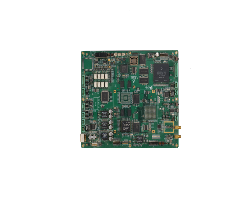
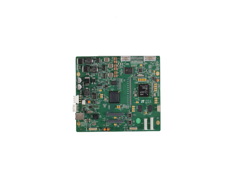
PCBs are the fundamental building blocks of most modern electronic devices. Semiconductors, resistors, capacitors, and diodes are all mounted on printed circuit boards to communicate with each other.
With the development of advanced technologies in recent years, the PCB manufacturing process has been fully automated, mainly including four steps: design, manufacturing, assembly, and testing.
PCB Design Process
As mentioned earlier, design is one step in PCB manufacturing. Typically, the PCB design process involves the following steps.
The recent COVID-19 pandemic did have some impact on the global PCB manufacturing industry, but with the increase in demand for electronic products and advancements in PCB manufacturing processes, the market is rapidly rebounding.
The global PCB market size is projected to increase from $70.92 billion in 2020 to $86.17 billion in 2026, with a Compound Annual Growth Rate (CAGR) of 3.3% from 2021 to 2026.
As a business owner or retailer, understanding the printed circuit board manufacturing process is necessary. This information can help you choose the right PCB manufacturer for your next project.
In this detailed guide, we will discuss the PCB manufacturing process, including design, testing, and assembly.
1. Schematic Design
Schematic design, also known as a schematic, is essentially the blueprint for designing a PCB. It provides a logical representation of the different PCB components, traces, and electronic circuits. Each component used on the board has an identifying symbol used to represent it on the schematic board.
● You need to have a clear understanding of what should be included in the PCB design, as the engineer will design the schematic based on your technical requirements.
● The designer will use logical symbols and notations for each component according to industry standards.
● Each symbol will have one or more pins connected by lines called nets to create the schematic design using CAD (Computer-Aided Design) software specifically for PCB design.
2. PCB Layout Planning
Once all the symbols are placed and the nets are connected in the schematic, the board can be physically designed, a process called "PCB layout," which includes:
● Creating models of the physical components in the layout tool.
● Ensuring that nets do not touch each other, otherwise they will short after the printed circuit board is built.
● Setting the physical shape and structure of the PCB in the layout database.
3. Component Placement Planning
Once the virtual schematic is ready, the next step in the PCB design process is to plan the component placement.
It will help you determine how many PCB layers are needed and other technical specifications.
Component placement also ensures that the board is manufactured without errors. This reduces the overall production cost of manufacturing the printed circuit board.
The designer will place the component packages in the following order.
● Fixed components such as connectors and switches are placed first in the layout database. This ensures that they match correctly with the plugs or openings in the system housing.
● Next, key components such as microprocessors, memory chips, and power supplies are placed next to the fixed components.
● Supporting components such as capacitors, resistors, and inductors will be placed near the key components.
● Finally, technicians will place PCB components such as termination resistors or large-capacity decoupling capacitors. They do not necessarily directly support the key components, but are essential in PCB manufacturing.
4. Route Connections
After the components are in place, the designer will use routing to connect the components.
In the PCB manufacturing process, routing will be transformed into component connections.
Four common track routing methods include:
● Manual routing: The designer selects a net and manually traces its routing. This is done by straight lines or curves, right angles, or by transitioning to another layer through a hole placed on the board called a via.
● Semi-automatic routing: Using the semi-automatic routing feature of the CAD application, the designer can route a net or group of nets.
● Automatic interactive routing: A combination of manual and automatic tracking, this feature allows the designer to manually create custom routing. But the CAD application will track it according to signal integrity rules.
● Batch automatic routing: The designer will manually trace all the routing and set the routing rules. They will first manually pre-route various areas and then use the autorouter to connect the nets.
5. Design the Board
At this stage of the PCB design process, the designer will use specialized applications called Electronic Design Automation (EDA) to plan and determine the number of layers, board size, and components.
● The designer will suggest PCB design changes based on your technical specifications and requirements, such as using surface mount instead of through-hole technology.
● Once the printed circuit board is complete, the designer will export the files in Gerber or CAD format according to industry standards.
6. Final Manufacturing Files
The final stage of the PCB design process involves exporting Gerber or CAD files for actual manufacturing. You can send these files along with the required set of instructions to the PCB board manufacturer.
PCB Manufacturing Process
PCB manufacturing or production begins after the PCB design is approved and the manufacturer receives the final manufacturing documents. At this point, your virtual circuit board design will become a physical printed circuit board.
1. Design Imagination
After multiple checks, your PCB board design is ready for printing. Your PCB board manufacturer uses a specialized printer called a plotter printer to convert the board design file into film. These films are like negatives of your schematic.
When printing, the inner layers of the PCB have two ink colors:
● Black ink represents the copper wires and circuits of the PCB.
● Transparent ink represents the non-conductive areas of the PCB, such as the fiberglass substrate.
The outer layers have:
● Transparent ink indicates copper paths
● Black ink indicates areas where copper will be etched away
The film also has alignment holes for aligning the printed circuit board at a later stage of the manufacturing process. The film will be stored in a safe place to avoid unnecessary contact.
2. Printing the inner layers on copper
This step in the PCB manufacturing process marks the beginning of the actual PCB manufacturing. The process starts with the basic shape of the PCB, which includes a laminate made of substrate material. The substrate material is usually epoxy resin and fiberglass.
● Print the PCB design onto the laminate
● Pre-bond copper to both sides of the laminate
● Then etch away the copper, following the PCB design shown on the film
● Next, cover the laminate with a photosensitive film called a resist
RECOMMENDED NEWS

High-end Custom Services: SMT Chip Processing Meets Diverse Industry Needs


(Telephone contact)
Email:
Address: Room 502, Building 1, No. 13, Bohua 4th Road, Huangpu District, Guangzhou City
COPYRIGHT © 2025 Guangzhou Tongsen Electronic Technology Co., Ltd. All rights reserved.