Welcome to Guangzhou Tongsen Electronic Technology Co., LTD. Website!


What is the difference between PCB and PCBA?
Double-sided and multilayer PCBAs offer numerous advantages, enabling designers to create highly complex circuits. Circuit designers have the freedom to choose the components and packages for their circuits. A common recommendation is to use at least one double-sided PCBA in a design to maintain simplicity and compactness.
PCB and PCBA are commonly used terms in the electronics manufacturing industry. Although these two abbreviations differ by only one letter, their meanings are vastly different; those outside the electronics industry may be ridiculed for improper use. What are the definitions of PCB and PCBA? What is the difference between PCBA and PCB?
Does the electronic device contain a PCB or a PCBA?
Taking a mobile phone as an example, let's disassemble it and look at the composition of its internal parts, mainly including the earpiece, speaker, microphone, battery, screen, keyboard, circuit board, and various chips.
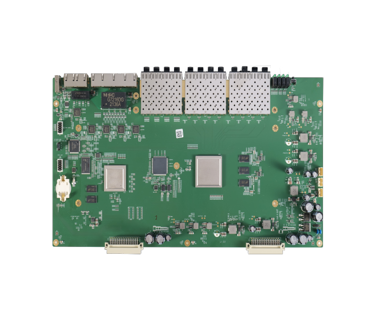
In the eyes of many electronic consumers, electronic products mainly rely on internal chips to function, which is correct, but they mistakenly believe that the entire green board is a chip. In many electronic products, the green board is one of the main characters of this article: the PCBA board. After disassembling the PCBA board, the bare PCB and electronic components can be obtained. Integrated circuits (ICs) or chips are a type of PCBA electronic component. The reason why we might confuse chips with PCBs and PCBAs is probably because chips are also called integrated circuits.
Breaking down the PCBA assembly process might help you distinguish these three relationships. Engineers program the required functions into the chip, then commission a PCBA company to manufacture and assemble the PCB. The circuit board obtained after assembly is the PCBA board. Therefore, the circuit boards in electronic devices sold on the market are called PCBA boards.
PCB vs. PCBA: A Comprehensive Comparison
After reading the above article, most people should now be able to distinguish between PCB and PCBA. Below, we will analyze and introduce these two terms from a more professional perspective, allowing everyone to better understand their differences.
What is a PCB?
A PCB is a crucial component of electronic circuits, not containing any integrated electronic components. It comprises several key elements, including the substrate, silkscreen, solder mask, conductive layers, pads, and vias. These elements collectively contribute to the PCB's functionality and integrity.
Upon its invention, the PCB was called a printed wiring board (PWB). To avoid unnecessary confusion/panic, PWB was renamed printed circuit board (PCB) because its name was associated with a toxic chemical.
Working Principle
The PCB is the foundation of modern electronic devices, an important electronic component, serving as both a support for electronic components and a carrier for their electrical connections. Almost all electronic devices, from electronic watches and calculators to computers, communication electronic equipment, and military weapon systems, contain PCBs.
A bare PCB, in isolation, does not possess any inherent function or purpose. However, once electronic components are meticulously assembled onto the board, the intricate wiring within the PCB becomes a crucial foundation, acting as a carrier for components and integrated circuits. It facilitates the necessary electrical interconnections between these components, enabling the seamless operation of the entire electronic system.
Main Types
Circuit boards have different types depending on different classification situations. Here are five common ways to distinguish PCBs:
Number of Layers: Single-layer (single-sided), double-layer (double-sided), multilayer PCBs, etc.
Flexibility: Flexible PCBs, rigid PCBs, rigid-flex PCBs, etc.
Substrate Material: Rogers, aluminum, ceramic, FR-4, etc.
Function: High-speed, HDI, high-frequency, etc.
Application: Military electronics, aerospace, consumer electronics, medical, etc.
What is PCBA?
PCBA is the abbreviation for Printed Circuit Board Assembly, representing the meticulous process of integrating electronic components onto a bare PCB using advanced assembly techniques such as SMT and THT. Therefore, the term PCBA board refers to a fully assembled circuit board containing integrated electronic components.
The CPU, as the brain of many electronic products, undertakes all signal transmission work, but it cannot work independently without the control of the PCB. Unlike the PCB, if the bare board is our body, then the PCBA circuit board is more like the human nervous system. As practitioners in the PCBA industry, we have always believed that PCBA is the core of electronic devices and the carrier of future technological development. This is because the lifespan, operating speed, reliability, and stability of consumer electronic products are directly related to the printed circuit.
Assembly Process
After the bare board is manufactured, it enters the assembly workshop. After SMT and THT processing, the PCB assembly process is completed.
SMT Assembly Process: Incoming inspection → Stencil printing solder paste → Chip placement → Drying → Reflow soldering → Cleaning → Inspection → Rework
THT Assembly Process: Incoming inspection → Manual insertion → Wave soldering → Trimming → Touch-up soldering → Cleaning → Functional testing → Rework
PCBA Cost Drivers
Compared to finished product costs, PCB assembly costs are more transparent and open. PCB assembly cost drivers = Material procurement (parts and bare boards) + Bare board manufacturing + PCB assembly (SMT and THT) + PCB testing + Transportation costs.
Combination of PCB and PCBA
After understanding the relationship between PCB and PCBA, let's take a double-layer PCB as an example to help everyone understand the process from PCB to PCBA.
There are many electronic components in electronic products, and these components are mounted on the circuit board. To make the circuit design more compact, electronic engineers usually use a double-layer or multi-layer structure, i.e., using more components in a smaller space. To this end, designers may use as many SMD packages as possible so that a large number of components can be placed on both sides. If the designer encounters any difficulties in routing, then he/she can use vias and/or transfer to another available layer to solve this problem. This makes the design process easier and more compact.
A double-sided PCB has plated-through holes for DIP components and plated pads for SMD packages, as well as component placement on both sides of the PCB. For soldered components using DIP packages, the flux will flow through the conductive plated-through hole and fill it, thereby securing the component leads passing through the hole. For SMD PCBAs, the flux simply forms a conductive layer on the SMD component leads and conductive pads in the PCB layout, and creates a path for current flow to create the circuit. After a tedious assembly process, the work from double-sided PCB to double-sided PCBA is completed.
Double-sided and multilayer PCBs offer numerous advantages, enabling designers to create highly complex circuits. Circuit designers have the autonomy to select the components and packages for their circuits. A common recommendation is to use at least one double-sided PCB in a design to maintain simplicity and compactness.
RECOMMENDED NEWS

High-end Custom Services: SMT Chip Processing Meets Diverse Industry Needs


(Telephone contact)
Email:
Address: Room 502, Building 1, No. 13, Bohua 4th Road, Huangpu District, Guangzhou City
COPYRIGHT © 2025 Guangzhou Tongsen Electronic Technology Co., Ltd. All rights reserved.