Welcome to Guangzhou Tongsen Electronic Technology Co., LTD. Website!


Functions and features of the backplane PCB
Adjacent signal layers should follow the principle of vertical routing. High-speed signal routing should avoid crossing reference planes. If it is necessary to cross reference planes, bypass capacitors should be placed in the gap between different reference planes to ensure signal impedance continuity and reduce signal reflection and crosstalk.
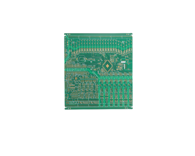
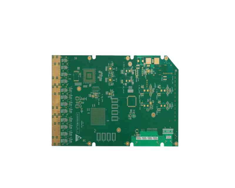
Backplane PCBs, also known as motherboards, are large, multi-layered, high-density printed circuit boards designed to meet the demands of complex systems. Compared to traditional PCBs, backplanes are larger, have more layers, and have a higher wiring density. They primarily serve to provide stable and efficient connections between various sub-boards, acting as the backbone network for system communication.
With the increasing complexity of IC components and the number of I/Os, as well as the rapid development of electronic assembly, high-frequency signal transmission, and high-speed digitization, the functions of backplanes are also constantly expanding, covering functions such as functional board support, signal transmission, and power distribution. To achieve these functions, the requirements for backplanes in terms of the number of layers (20-60 layers), board thickness (4-12mm), the number of vias (30,000-100,000), reliability, frequency, and signal transmission quality are becoming increasingly stringent.
What are the main functions of a backplane PCB?
Mechanical Support
Backplane PCBs provide a stable foundation for electronic devices, offering mechanical support and securing internal components to ensure stability and safety.
Electrical Connection
The complex circuit network on the backplane PCB connects various electronic components, chips, modules, and other devices, facilitating electrical connections and communication within the device.
Signal Transmission
Backplane PCBs are responsible for transmitting high-speed signals and data, ensuring fast and stable communication between components, thereby guaranteeing the normal operation of electronic devices.
Power Distribution
Backplane PCBs manage power distribution, ensuring that all components receive a stable and reliable power supply to meet the device's power consumption needs.
Thermal Management
Backplane PCBs conduct and dissipate heat, helping to effectively release internal heat and prevent electronic components from being damaged by overheating.
EMI/EMC Control
The design of backplane PCBs fully considers electromagnetic interference (EMI) and electromagnetic compatibility (EMC), taking measures to minimize the device's interference with the external environment, ensuring stability and reliability.
Backplane PCBs play a crucial role in the connection, support, transmission, and management within electronic devices, directly affecting the performance, stability, and reliability of the electronic equipment.
Features and Advantages of Backplane PCBs
Maintainability
The design of backplane PCBs fully considers the convenience of maintenance and repair, using modular design and standard interfaces for easy replacement and repair. For example, industrial control system backplanes use a modular design, allowing for quick replacement of faulty modules, thus reducing maintenance time and costs.
Enhanced Stability Backplane PCBs use high-quality materials and advanced manufacturing processes to ensure their stability and reliability, maintaining excellent performance even in harsh environments. For example, military equipment backplanes use highly reliable materials and processes, undergoing rigorous testing and verification to ensure stability and reliability under battlefield conditions.
Assemblability
The design of backplane PCBs fully considers the needs of assembly and integration, allowing for flexible combination with other components to meet the design requirements of various devices. For example, industrial automation equipment backplanes can be flexibly combined with various sensors, actuators, and other components to achieve complex control functions.
High-Density Capability
Backplane PCBs have the advantage of high-density wiring, capable of transmitting and processing large amounts of signals in a limited space, meeting the high requirements of modern electronic devices for data transmission speed and processing capacity. For example, server backplanes use high-density wiring design to achieve high-speed transmission and processing of large amounts of data.
Functionality
Backplane PCBs can integrate various functions and communication interfaces to meet the functional needs of different devices. For example, industrial control system backplanes integrate multiple communication interfaces and control functions to achieve complex control and monitoring functions.
Material Selection and Layer Stack Design for Backplanes
Backplane Material Selection
Backplanes typically use FR4-TG170 or higher grade materials. Compared to standard FR4-TG130, these materials have a higher glass transition temperature and better flame retardancy. Materials with a dielectric constant ε (Dk) of no more than 4.4 are usually chosen to reduce signal crosstalk.
Backplane Layer Stack Design Principles
The layer stack design of backplane PCBs should follow the following principles:
Layer Stack Principles:
Backplane PCBs typically include signal layers, power layers, and ground layers. The ground and power layers can provide a low-impedance return path for adjacent signal traces. Signal layers should be located between power or ground reference layers, forming a symmetrical stripline or asymmetrical stripline structure.
Power Domain Division:
Backplanes have multiple power supplies, such as -48V, 12V, 3.3V, etc. The number of layers for each power supply's traces should be determined based on current requirements. The power layers need to be tightly coupled with the ground layers to reduce common-mode EMI interference.
Signal Layers:
Adjacent signal layers should follow the vertical routing principle. High-speed signal traces should avoid crossing reference planes. If they must cross reference planes, bypass capacitors should be placed in the gap between different reference planes to ensure signal impedance continuity and reduce signal reflection and crosstalk.
Ground Planes:
Include as many ground planes as possible to provide a low-impedance return path. Consider using thin prepreg (PP) to enhance coupling between the ground plane and signal layers or other ground planes.
Maintain Layer Stack Symmetry:
Try to make the signal layers, power layers, and ground layers symmetrical. If a signal layer corresponds to a power layer or ground layer, cover the unused area of the signal layer with ground copper to maintain symmetry and prevent warping during manufacturing.
Key Points in Manufacturing Backplane PCBs
1. Material Selection and Thickness Control
Backplane PCBs are generally thicker and heavier than standard PCBs, so the requirements for material selection and thickness control are stricter. Selecting appropriate substrates and copper clad laminates, such as FR-4, FR-5, high-TG materials, etc., and strictly controlling the thickness can ensure the mechanical strength, thermal stability, and electrical performance of the backplane PCB. In addition, considering the coefficient of thermal expansion of the material is also important to avoid deformation or stress concentration due to temperature changes, thus ensuring the stability and reliability of the circuit.
2. Layer Alignment
Due to the high number of layers and drill holes in the backplane PCB, layer alignment is a crucial manufacturing process. High-precision lamination technology and advanced alignment equipment are used to ensure the accuracy and stability of layer alignment.
3. Special Process Handling
Backplane PCB manufacturing involves special processes such as electroless copper plating, surface treatment, lamination, drilling, and electroplating. These processes must be strictly controlled to ensure the quality and stability of the backplane.
4. Thermal Management and Heat Dissipation Design
Due to the significant thickness and weight of the backplane PCB, thermal management and heat dissipation are critical issues in the manufacturing process. Heat sinks, thermal pads, fans, and heat pipes, along with suitable heat dissipation materials such as copper, aluminum, and thermal grease, can improve the heat dissipation efficiency of the backplane PCB. Thermal simulation and testing to evaluate the effectiveness of the heat dissipation design ensure the stability and reliability of the backplane PCB.
5. Process Monitoring and Quality Control
Strict process monitoring and quality control are essential for backplane PCB manufacturing. This involves detailed process specifications, regular maintenance and calibration of production equipment, rigorous process parameter control, real-time monitoring and adjustment of the manufacturing process, and rigorous inspection and testing of raw materials, processes, and finished products. This ensures that each step and stage meets the design requirements and standards, ensuring a stable and reliable manufacturing process that produces products that meet design requirements and standards, enhancing product competitiveness and market share.
Conclusion
With the development of technologies such as 5G, the Internet of Things, and artificial intelligence, backplane PCBs will continue to evolve. To meet the needs of higher data transmission speeds and more complex system integration, backplane PCBs will adopt more advanced materials and manufacturing processes, such as high-frequency materials and microwave-level manufacturing technologies. Furthermore, as electronic devices move towards miniaturization and high performance, backplane PCB design will increasingly focus on thermal management and signal integrity, while incorporating modular design concepts to improve system flexibility and scalability. These trends will drive the widespread application of backplane PCBs in communications, data centers, and smart devices.
Previous :
RECOMMENDED NEWS

High-end Custom Services: SMT Chip Processing Meets Diverse Industry Needs


(Telephone contact)
Email:
Address: Room 502, Building 1, No. 13, Bohua 4th Road, Huangpu District, Guangzhou City
COPYRIGHT © 2025 Guangzhou Tongsen Electronic Technology Co., Ltd. All rights reserved.