Welcome to Guangzhou Tongsen Electronic Technology Co., LTD. Website!


SMT Assembly: Frequently Asked Questions
X-ray inspection: This test is part of the standard inspection for lead-free components (such as ball grid arrays and related quad flat packages) in PCB manufacturing. It provides an X-ray image of components and solder joints that are not visible to the operator.
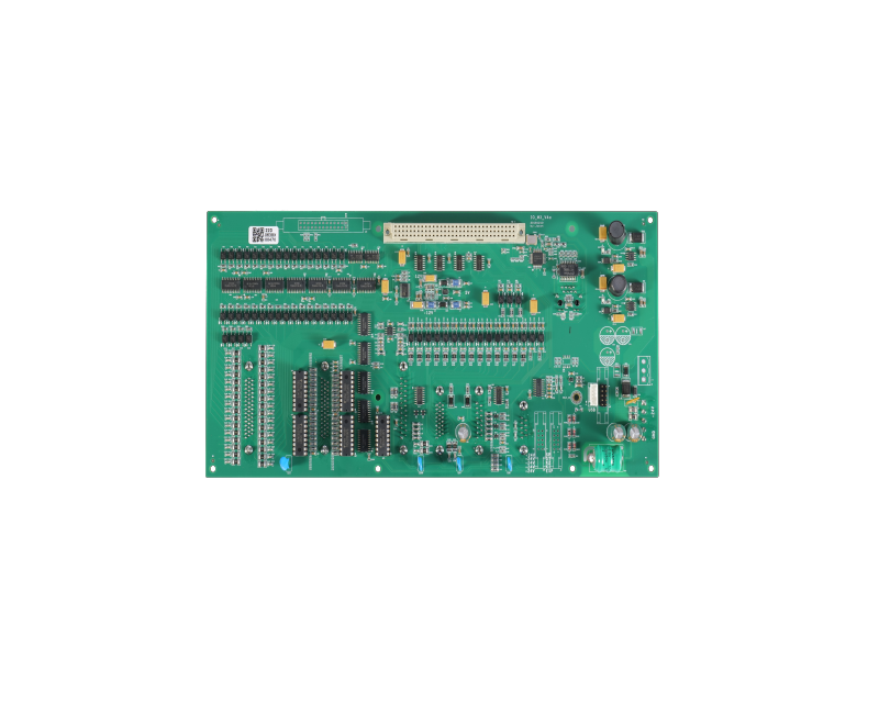
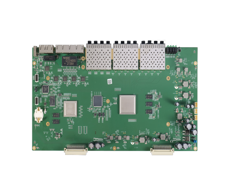
SMT is a surface mount technology used for assembling and packaging parts by placing and soldering components directly onto the surface of a PCB. This technology helps reduce manufacturing costs and improve efficiency. The process also enables the construction of highly complex electronic circuits in smaller components using automated methods. SMT assembly provides a high degree of circuit reliability and space utilization in circuit boards. PCBs are the backbone of all electronic circuits and can be assembled in rigid, flexible, or rigid-flex forms depending on the design.
What techniques are used in SMT assembly?
The techniques vary depending on the soldering method and assembly style. Traditional PTH (plated through-hole) assembly is done by hand soldering or using a wave soldering machine. In this case, holes are drilled in the PCB for component mounting, and solder is drawn into the holes to complete the circuit connection.
SMT technology aims to solder components to connection pads embedded on the surface of the PCB. Solder paste containing flux is screen-printed onto these pads, and then the components are heated and cooled using a reflow oven, forming solder joints that complete the circuit connection. In SMT, there are single-sided, double-sided, and mixed technology approaches, allowing the combination of SMT and PTH on the same board.
What are the benefits of SMT assembly?
Compared to the older through-hole technology, SMT offers many advantages, including:
SMT assembly requires fewer holes to be drilled in the PCB, saving time. EMC performance is also better due to the smaller radiation loop area and lead inductance.
SMT assembly has lower initial setup costs, making it suitable for mass production and automation.
It involves smaller components and higher component density per unit area.
Components in SMT assembly can be placed on both sides of the board.
In SMT assembly, small errors in component placement are automatically corrected. The molten solder pulls the component into alignment with the pad, unlike through-hole assembly where components may be slightly misaligned.
SMT assembly has better mechanical performance and lower resistance under vibration conditions, unlike through-hole components, giving it better predictable high-frequency performance.
What are the different types of SMT?
SMT assembly types include:
Ball Grid Array (BGA)
Ultra Fine Pitch Ball Grid Array
Quad Flat Package (QFP)
Quad Flat No-Lead Package (QFN)
Small Outline Integrated Circuit (SOIC)
Plastic Leaded Chip Carrier (PLCC)
Populated Package (POP)
Small Outline Package (SOP)
How is the SMT process completed?
The SMT process begins with the design phase, where various components are selected, and the PCB is designed using one of the software platforms such as PADS. All design features are included in this phase, and the PCB layout is defined. Key considerations for incorporating PCB functionality are made, and components are selected for the next phase. The PCB data is then prepared, and the manufacturing process can begin.
Machine Programming
The next step is setting up the machines for the manufacturing process. A program with CAD-generated data is developed for the pick-and-place machines and automated optical inspection to assist with SMT assembly.
Solder Paste Printing
The solder paste printer is then programmed to apply solder paste to the pads of the printed circuit board via a stencil. The stencil design is very carefully considered as solder paste application is a critical process that needs careful consideration to eliminate printing and downstream soldering defects.
Solder Paste Inspection
Solder paste printers have automatic inspection capabilities, depending on the size of the PCB, other printers have a separate inspection machine. The inspection machine uses 3D technology for comprehensive inspection, this type of inspection is better and more popular as it can inspect the solder paste volume on each pad, not just the volume within the printed area.
Component Placement
Solder paste printers have automatic inspection capabilities, depending on the size of the PCB, other printers have a separate inspection machine. The inspection machine uses 3D technology for comprehensive inspection, this type of inspection is better and more popular as it can inspect the solder paste volume on each pad, not just the volume within the printed area.
Automated Optical Inspection (AOI) Before Reflow
After component placement, verification is done through automated optical inspection to ensure that the components are placed in the correct location. This is done using an AOI machine that checks for component presence, value, and polarity.
Reflow Soldering
This process occurs after all the electrical solder connections are made between the components and the PCB. This process is done by heating the PCB assembly to a sufficient temperature to form acceptable solder joints.
Following this, post-reflow automated optical inspection is performed to ensure there are no errors, and then X-ray inspection is used for process verification.
What is the turnaround time for turnkey orders in SMT assembly?
Turnaround time depends primarily on the speed of obtaining all the PCB parts so that SMT assembly can begin.
What different testing services are performed during SMT assembly?
During SMT assembly, the following are performed:
Automated Optical Inspection (AOI): AOI can be used pre- or post-soldering to help identify component presence, placement, and solder quality.
X-Ray Inspection: This test is part of the standard inspection of lead-free components such as ball grid arrays and related quad flat packages in PCB manufacturing. It provides an X-ray image of the components and solder joints that are not visible to the operator.
In-Circuit Testing: The purpose of the test is to check for any shorts or joint failures. Testing is done through an ICT platform and a bed-of-nails or customer fixture designed for the components to be tested.
Functional Testing: Functional checks are performed to ensure that the PCB works efficiently and meets requirements after SMT assembly.
Next :
RECOMMENDED NEWS

High-end Custom Services: SMT Chip Processing Meets Diverse Industry Needs


(Telephone contact)
Email:
Address: Room 502, Building 1, No. 13, Bohua 4th Road, Huangpu District, Guangzhou City
COPYRIGHT © 2025 Guangzhou Tongsen Electronic Technology Co., Ltd. All rights reserved.