Welcome to Guangzhou Tongsen Electronic Technology Co., LTD. Website!


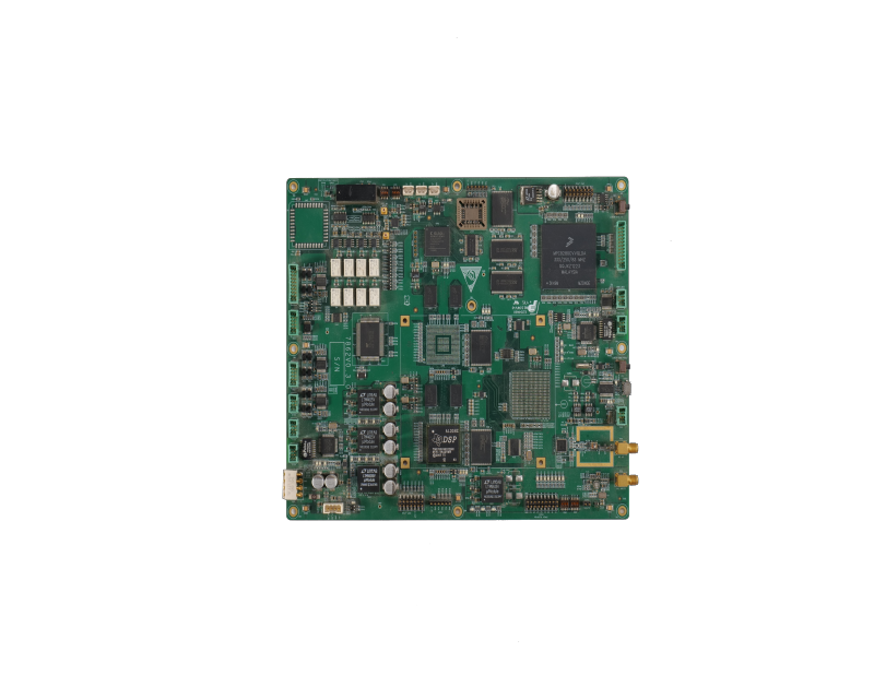
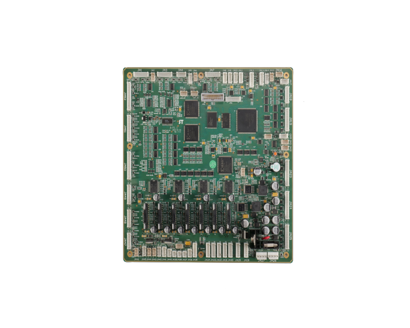
SMT Assembly Process Guide
Passed products are separated and packaged. Commonly used packaging materials include bubble film, anti-static cotton, and blister trays. There are two main packaging methods. The first is to use bubble film or anti-static cotton in rolls for separate packaging, which is currently the most common packaging method; the second is to place the PCBA in a custom-sized blister tray, mainly for PCBAs with sensitive needles and easily damaged SMD components.
In the era of rapid development of electronic products, the design and manufacturing processes of electronic products are also developing rapidly, and an important technology is PCB manufacturing. SMT, as an important process in electronic circuit board processing, lays the foundation for the processing and production of circuit boards. In this article, we will discuss in detail what SMT is.
What is SMT?
SMT, or Surface Mount Technology, is one of the popular technologies and processes in the electronics assembly industry,
It is an electronic assembly technology that mounts surface mount devices without leads or with short leads onto the surface of a printed circuit board or other substrate and solders them to the assembly using reflow soldering.
Why choose SMT?
SMT, or Surface Mount Technology, is a popular technology and process in the electronics assembly industry. It mounts surface mount devices without leads or with short leads onto the surface of a printed circuit board or other substrate, using reflow soldering or dip soldering to solder the components. Surface mount components; at the same time, production, product batching, and production automation enable manufacturers to achieve high yields at low costs, produce high-quality products, meet customer needs, and enhance market competitiveness. On the other hand, the development of electronic components, integrated circuits, and the diversified application of semiconductor materials have also promoted the development of SMT.
Background of SMT
1. Electronic products pursue miniaturization, and the components using through-hole plug-in are no longer sufficient for size reduction. Electronic products are becoming increasingly integrated, using through-hole-free integrated circuits, especially large-scale, highly integrated ICs, which require the use of surface mount components—product batching, production automation, low cost, high yield, to obtain high-quality products, meet customer needs, and enhance market competitiveness.
2. Development of electronic components, integrated circuits (ICs), and diverse applications of semiconductor materials.
Advantages of SMT
1. High assembly density, small size, and light weight of electronic products. The volume and weight of surface mount components are only about one-tenth of traditional plug-in components. Generally, after using SMT, the volume of electronic products is reduced by 40%~60%, and the weight is reduced by 60%~80%.
2. High reliability, strong impact resistance, and low solder joint defect rate.
3. Good high-frequency characteristics, reducing electromagnetic and radio frequency interference.
4. Easy to achieve automation, improve production efficiency, reduce costs by 30%~50%, saving materials, energy, equipment, manpower, time, and space.
Quick understanding of the SMT process flow
1. Programming and adjusting the display
According to the customer-provided sample BOM and placement map, a scheme for the position coordinates of the surface mount components is created. Then, combined with the SMT placement processing information provided by the customer, the first-piece processing is carried out.
2. Solder paste printing
The solder paste is screened onto the SMD pads of the PCB board where the electronic components need to be soldered using a steel mesh, preparing for the soldering of the components. The equipment is a screen printing machine (transfer printing machine), located at the front end of the SMT placement processing production line.
3. SPI
Solder paste inspection instrument, testing whether the solder paste printing is good, whether there are any defects such as insufficient solder, missing solder, or excessive solder.
4. SMD
Accurately mount the SMD electronic components to the fixed positions on the PCB. The equipment used by the placement machine is located on the SMT production line, behind the screen printing machine. Placement machines are divided into high-speed machines and general-purpose machines. High-speed machines are used for mounting small components with small lead spacing.
General-purpose machine: Pasting components with small lead spacing (high lead density) and large size.
5. High-temperature solder paste melting
Mainly, the solder paste is melted at a high temperature and cooled to firmly solder the SMD electronic components to the PCB board. The equipment used is a reflow soldering furnace, located behind the placement machine in the SMT production line.
6.AOI
Automatic Optical Inspection (AOI), detects whether there are any soldering defects such as marks, displacement, or empty soldering after the components are soldered.
7. Visual inspection
Manual inspection focuses on checking the following items: Whether the PCBA version is a modified version; whether the components use substitute materials or brands as required by the customer; whether the direction of ICs, diodes, transistors, tantalum capacitors, aluminum capacitors, switches, etc., is correct; soldering defects: short circuits, open circuits, false components, and cold soldering.
8. Packaging
The tested products are separated and packaged. The commonly used packaging materials are bubble film, anti-static cotton, and blister trays. There are two main packaging methods. One is to use bubble film or anti-static cotton in rolls for separate packaging, which is the most commonly used packaging method; the other is to place the PCBA in a custom-sized blister tray, mainly for PCBA boards with sensitive needles and easily damaged SMD components.
RECOMMENDED NEWS

High-end Custom Services: SMT Chip Processing Meets Diverse Industry Needs


(Telephone contact)
Email:
Address: Room 502, Building 1, No. 13, Bohua 4th Road, Huangpu District, Guangzhou City
COPYRIGHT © 2025 Guangzhou Tongsen Electronic Technology Co., Ltd. All rights reserved.