Welcome to Guangzhou Tongsen Electronic Technology Co., LTD. Website!


PCB Material Selection Guide
Through-holes are typically filled with Ball Grid Array (BGA) components. If the BGA pins contact the inner layer, solder may slide through the through-hole to another layer. Therefore, through-holes need to be filled to ensure that solder does not leak to another layer and maintain the integrity of the contact as expected.
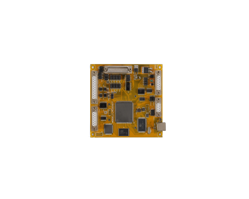
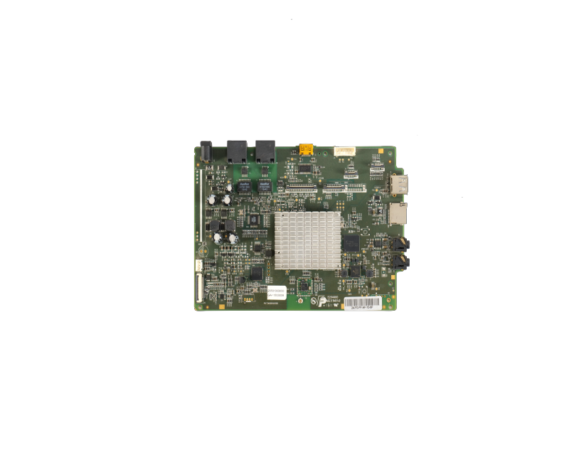
PCBs are an important part of electronic products. Additionally, the abbreviation also refers to Printed Circuit Boards and Printed Circuit Cards, which are essentially the same thing. Because these boards play a crucial role in a variety of devices ranging from computers to calculators, care should be taken in selecting PCB materials and understanding the electrical needs of the specific device.
Before the advent of PCBs, circuit boards were largely populated with wires that were wound together and overlapped, making them prone to failure at certain connection points. Over time, some wires would break, and they could also short-circuit. One can imagine that the wiring process for these early circuit boards was extremely complex and laborious.
As more and more everyday electronic components began to rely on circuit boards, a race began to develop simpler and more compact alternatives, leading to the development of PCB materials. Using PCB materials, circuits could be routed between many different components. The metal that facilitates the current transfer between the board and any connecting components is called solder, which also serves a dual purpose, having adhesive properties.
PCB Material Composition
PCBs are typically composed of four layers that are pressed together using heat to form a single unit. The different types of PCB materials used in a PCB from top to bottom include the silkscreen, solder mask, copper, and substrate.
The final layer is the substrate, made of fiberglass, also known as FR4. The letters FR stand for "flame retardant." This substrate layer provides a solid foundation for the PCB, but the thickness can vary depending on the intended use of the specific board.
There are also cheaper boards on the market that do not use the aforementioned PCB substrate material, instead being made of phenolic or epoxy resin. Due to the heat sensitivity of these boards, they tend to be prone to delamination. These cheaper boards are often easily identifiable by the smell they give off when soldered.
The second layer of a PCB is copper, pressed onto the substrate using a mixture of heat and adhesive. The copper layer is thin, and some boards have two layers of copper—one above and one below the substrate. PCBs with only one layer of copper are typically used in cheaper electronic devices.
Currently, a large number of copper clad laminates (CCL) used are categorized into different types according to different classification standards such as reinforcing materials, resin adhesives used, flammability, and CCL performance.
Above the green solder mask is the silkscreen layer, which has letter and number indicators added to it, allowing the technical programmer to read the PCB. This, in turn, makes it easier for the electronics assembler to place each PCB in the correct location and orientation on each component. The silkscreen layer is typically white, but colors such as red, yellow, gray, and black are sometimes used.
Other PCB Design Considerations
Numbers such as 1.6 mm are used to denote the thickness of the board. For a 4-layer board, 1.6 mm is a standard measurement. For example, a thicker board will provide more support when heavier connecting objects need to be supported.
The standard level for copper thickness on the planar layer is 35 micrometers. Alternatively, copper thickness is sometimes expressed in ounces or grams. Above-normal levels of copper thickness are employed on circuit boards that support a large number of applications.
Traces are not intended to carry power, but this sometimes happens when signals cannot properly handle the frequency. If this problem is not controlled, the trace may eventually lose a significant amount of power. To transfer as much power as possible from one side of the trace to the other, the layout of the trace must take into account the transmission equation.
Generally, on boards made of copper trace FR4 PCB material, two inches is a suitable trace distance, provided the signal time is one nanosecond. However, you must consider the effect of transmission lines on high trace lengths, especially when signal integrity is critical. The internet is full of programs and spreadsheets designed to help people make the correct impedance calculations for their specific board.
In most boards, vias are empty and can usually be seen directly. Nevertheless, vias can be filled in various situations. First, vias must be filled when a protective barrier against dust and other impurities is needed. Second, filling vias may be done to improve current carrying capacity, in which case a conductive material may be used. Another reason for filling vias is to make the board more planar.
Vias are commonly filled with ball grid array (BGA) components. If the BGA pins make contact with the inner layer, solder may slide through the via to another layer. Therefore, vias need to be filled to ensure that the solder does not leak to another layer and maintains the integrity of the contact as intended.
One of the troublesome situations on a board is when a contact intermittently breaks at a certain point on the board. The more often this happens, the more likely that part of the board will fail completely. This problem is encountered by the average home electronics user when a button on a calculator stops working. Each button presses a specific part of the board, and when a point fails, the button associated with that point cannot send a signal.
Another way contacts can wear out in places is by having an auxiliary card slot on the main board. If the card is mishandled, a point on the card may be damaged and will no longer work. A better way to protect the surfaces of the boards that come into contact with each other is to use a gold layer, which can act as a barrier to extend the lifespan. However, gold can be expensive, and using gold in the contacts adds another step in the PCB manufacturing process.
Previous :
Next :
RECOMMENDED NEWS

High-end Custom Services: SMT Chip Processing Meets Diverse Industry Needs


(Telephone contact)
Email:
Address: Room 502, Building 1, No. 13, Bohua 4th Road, Huangpu District, Guangzhou City
COPYRIGHT © 2025 Guangzhou Tongsen Electronic Technology Co., Ltd. All rights reserved.