Welcome to Guangzhou Tongsen Electronic Technology Co., LTD. Website!


What is the SMT process flow? Check the SMT process introduction
SMT process refers to Surface Mount Technology, which is the processing and welding of components on the basis of a printed circuit board (PCB), abbreviated as SMT. It is currently a popular electronic product processing and welding technology.
The SMT process refers to Surface Mount Technology, a process of component processing and soldering on a printed circuit board (PCB), abbreviated as SMT. It is currently a popular electronic product processing and soldering technology. The basic SMT process includes solder paste printing, electronic component placement, reflow soldering, AOI optical solder joint inspection, X-ray inspection, repair, and cleaning. Today's electronic products increasingly pursue miniaturization, and the plug-in method can no longer meet the current situation, so surface mount technology (SMT) must be adopted. Today, let's introduce the SMT surface mount processing flow.
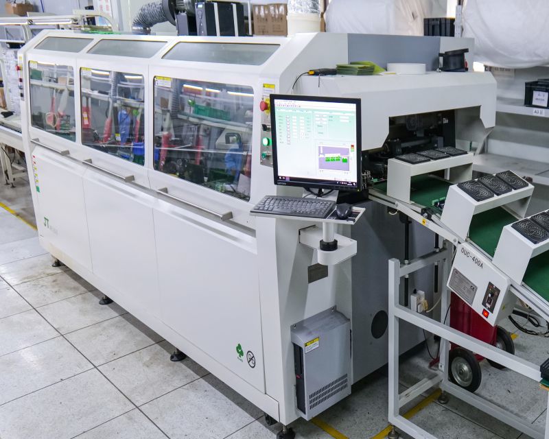
Abstract: I. The basic processes of SMT surface mount processing include: solder paste printing (red glue printing), SPI, chip placement, first-piece inspection, reflow soldering, AOI inspection, X-ray, rework, and cleaning. The function of each process is explained below.

Solder Paste Printing:
First, fix the circuit board that needs to be printed on the printing positioning table. Then, use the front and rear doctor blades of the printing machine to transfer the solder paste or red glue through the stencil to the corresponding PCB pads. The evenly printed PCB is then fed to the next process via a transfer table. Both solder paste and chips have thixotropy and viscosity. When the solder paste printer moves forward at a certain speed and angle, it will exert a certain pressure on the solder paste, pushing the solder paste to roll in front of the doctor blade, creating the pressure needed to inject or print the solder paste. The viscous frictional force of the solder paste causes shear at the connection between the doctor blade and the stencil of the solder paste printer. This shear force reduces the viscosity of the solder paste, facilitating the smooth injection and printing of the solder paste.
SPI:
SPI plays a very important role in the entire SMT surface mount process. It is a fully automatic non-contact measurement used after the solder printer and before the chip placement machine. Relying on structural light measurement and display (mainstream) or laser measurement (non-mainstream) technologies, it performs 2D or 3D measurement (micrometer-level accuracy) of PCB solder printing. The principle of structural light measurement products: A high-speed CCD camera is set in the vertical direction of the object (PCB and solder paste). A projector irradiates periodic striped light or images from an oblique upward direction to the object. When there are high-position components on the PCB, a displaced image of the stripes relative to the base plane will be captured. Using the triangulation principle, the offset value is converted into a degree value.
Pick and Place Machine
The chip placement machine is configured after the SPI. It is a device that uses a moving mounting head to accurately place surface mount components on the PCB pads. It is a device that achieves high-speed and high-precision mounting of components and is a key and complex device in the entire SMT surface mount processing production.
Reflow Soldering
Reflow soldering is the process of re-melting the solder paste pre-distributed on the PCB pads to achieve a mechanical and electrical connection between the welding ends or pins of the surface mount components and the PCB pads. The reflow soldering machine used in the reflow soldering process is located at the end of the SMT production line.
Optical Inspection
Using the principle of light reflection, and the different reflection capabilities of copper and the substrate to light to form a scanning image, the standard image is compared and analyzed with the actual layer image to determine whether the detected object is OK.
X-ray
The X-ray inspection equipment uses X-rays to penetrate the PCBA being inspected and then maps the X-ray image onto the image detector. The imaging quality is mainly determined by the resolution and contrast. This equipment is generally placed in a separate room in the SMT workshop.
Rework
Repairing the solder joint defects of the PCB board detected by AOI. The tools used include soldering irons, hot air guns, etc. The rework station can be configured at any position on the production line.
Cleaning
Cleaning mainly removes the flux residue from the processed PCBA board. The equipment used is a cleaning machine, fixed at the back end of the production line or in the packaging area.
Next :
RECOMMENDED NEWS

High-end Custom Services: SMT Chip Processing Meets Diverse Industry Needs


(Telephone contact)
Email:
Address: Room 502, Building 1, No. 13, Bohua 4th Road, Huangpu District, Guangzhou City
COPYRIGHT © 2025 Guangzhou Tongsen Electronic Technology Co., Ltd. All rights reserved.