Welcome to Guangzhou Tongsen Electronic Technology Co., LTD. Website!


What is the PCBA manufacturing process?
If you order one-stop PCB assembly, the PCB company will manufacture the PCB. During the PCB manufacturing process, SMT stencils for PCB assembly will also be manufactured. PCB manufacturing takes time, and the specific time depends on the complexity of the circuit board. At PCBONLINE, the short manufacturing cycle for PCB prototypes is 12 hours.
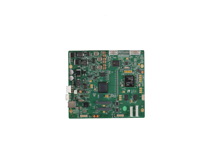
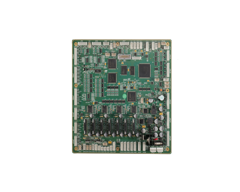
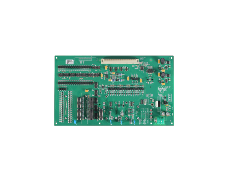
PCBA manufacturing is the process of assembling blank printed circuit boards. You can learn about the PCBA manufacturing process of a PCB factory below.
PCBA Sample Manufacturing Process
Before mass PCBA manufacturing, a complete PCBA sample needs to be made to check if every step and detail is perfect.
Step 1. Check the Bill of Materials (BOM) and Gerber files
The BOM is an Excel file containing all component requirements. Responsible PCB companies usually check your BOM and Gerber files to ensure there are no problems with your design before quoting you.
Step 2. Manufacture the PCB and SMT stencils for PCB assembly
If you order one-stop PCB assembly, the PCB company will manufacture the PCB. During PCB manufacturing, SMT stencils for PCB assembly will also be manufactured. PCB manufacturing takes time, depending on the complexity of the board. At PCBONLINE, the short manufacturing cycle for PCB prototypes is 12 hours.
Step 3. PCBA First Article Inspection
First Article Inspection (FAT) is a necessary condition for mass production of PCBAs, because once a small error occurs, the entire batch of PCBAs will be unqualified. Usually, the PCBA factory will produce 5 PCBAs, and one of them will be randomly selected for testing.
Technicians use probes to contact each component on the PCBA. The FAT machine receives and analyzes the returned data such as resistance and voltage. The computer displays the test results visually and audibly. If the PCBA is good, the computer will say "correct". If not, it will say "error".
After the FAT is completed, a test report will be generated for customer review. If the customer thinks the production effect is good and agrees to mass produce the PCBA, then the PCBA manufacturer will start mass production.
Complete Process of Mass PCBA Manufacturing
Step 1. Solder Paste Printing
Circuit boards are processed one by one by the pick-and-place machine. The pick-and-place stencil is set on the pick-and-place machine, with the PCB at the bottom of the stencil. The pick-and-place machine's blade carrying the solder paste presses against the PCB stencil, and the solder paste is applied through the stencil holes onto the PCB pads. When the circuit board is finished, it leaves the pick-and-place machine, and the next board enters the machine.
Step 2. Solder Paste Inspection (SPI)
The standard solder paste thickness ranges from 0.09mm to 0.15mm, and the solder paste must completely cover the PCB pads. The PCB enters the SPI machine, and the machine checks whether the solder paste thickness and shape meet the PCB assembly requirements.
Step 3. High-Speed Mounting
When the PCB enters the high-speed pick-and-place machine, the robot picks up smaller SMD components at a high speed and places them on the required PCB pads. These SMDs have package sizes of 0201, 0402, and 0603. For example, fasteners, resistors, and capacitors. After the high-speed pick-and-place machine completes the placement operation, the PCB with SMDs leaves the high-speed pick-and-place machine, and the next bare PCB enters.
Step 4. Functional Mounting
Larger SMD components have package sizes of 0804 and above, such as BGAs, FPGAs, ICs, USBs, etc. Like the high-speed pick-and-place machine, these SMDs are also prepared before PCBA manufacturing. In the functional pick-and-place machine, the robot picks and places the SMDs onto the required pads according to the set program, but the operation speed is much slower and more accurate. Then the PCBA leaves the functional pick-and-place machine. It must pass solder paste inspection (SPI) to ensure that the solder paste thickness and shape on the pads are qualified.
Step 5. X-Ray
When all SMDs are mounted, the PCBA undergoes X-ray testing. After the X-ray penetrates the PCBA, an image is generated on the machine screen, and the technician judges whether the PCBA is qualified based on the test results.
Step 6. Reflow Soldering
In this step, the PCBA passes through the reflow oven, and the solder paste melts and solidifies. The reflow oven has different temperature zones, and the temperature is controlled. Usually, in one temperature zone, the PCBA is preheated. In the middle, the solder paste melts completely. In the subsequent temperature zones, the solder paste gradually cools and solidifies. After reflow soldering, the SMDs are tightly soldered to the PCB pads.
Step 7. Automated Optical Inspection (AOI)
After reflow soldering, the PCBA needs to go through the AOI machine. The camera automatically scans the PCBA, the AOI machine collects images, compares the detected solder joints with the set parameters in the database, checks for defects on the PCB through image processing, and marks the defects on the screen. If there are defects, the quality control personnel mark the defects on the circuit board for repair.
Step 8. Through-Hole (PTH) Assembly
PTH assembly is the process of mounting PTH components onto the PCBA. The pins of PTH components are much longer than SMD components, and the pins must pass through the PCB through-holes. This operation is quite simple and is usually done manually.
Step 9. Wave Soldering
After PTH assembly, there are still gaps between the PTH pins and the PCBA. Wave soldering fills the gaps, making the PTH components tightly connected to the PCBA.
After the PCBA is preheated by the preheater, it passes through the wave soldering furnace. In the furnace, liquid tin fills the gaps between the PTH pins and the PCBA. When the PCBA leaves the furnace, the tin cools and solidifies. In this way, the PTH components are firmly connected to the PCBA.
Step 10. Trim PTH Pins and Fix PCBA
In this step, first, a technician trims the PTH pins to a length of 1 to 2 millimeters. If any soldering is imperfect, another technician will use a soldering iron to fix the PCBA.
Step 11. Conformal Coating
This step is optional. Conformal coating is automatically sprayed onto the surface of the PCBA to protect the PCBA from moisture, dust, chemicals, vibration, etc.
Step 12. PCBA Functional Test (FCT)
The technician picks up the PCBA on the FCT fixture, turns on the power, and the functional tester performs tests such as current and voltage. The test results are displayed on the computer screen.
Step 13. Thermal Aging Test
Place the PCBA in a thermal chamber and power it on continuously for about 250 hours. The temperature is raised to a certain level. All PCBAs should follow the ECIA-EIA-364-17 standard.
Additional PCBA testing can be added to the PCB assembly steps described above. For PCBs used in aerospace, defense, automotive, medical, and communication applications, PCBA manufacturing also requires four-point sensing. In addition, flying probe testing, in-circuit testing, IC programming, and repairs (as needed) may also be performed.
RECOMMENDED NEWS

High-end Custom Services: SMT Chip Processing Meets Diverse Industry Needs


(Telephone contact)
Email:
Address: Room 502, Building 1, No. 13, Bohua 4th Road, Huangpu District, Guangzhou City
COPYRIGHT © 2025 Guangzhou Tongsen Electronic Technology Co., Ltd. All rights reserved.