Welcome to Guangzhou Tongsen Electronic Technology Co., LTD. Website!


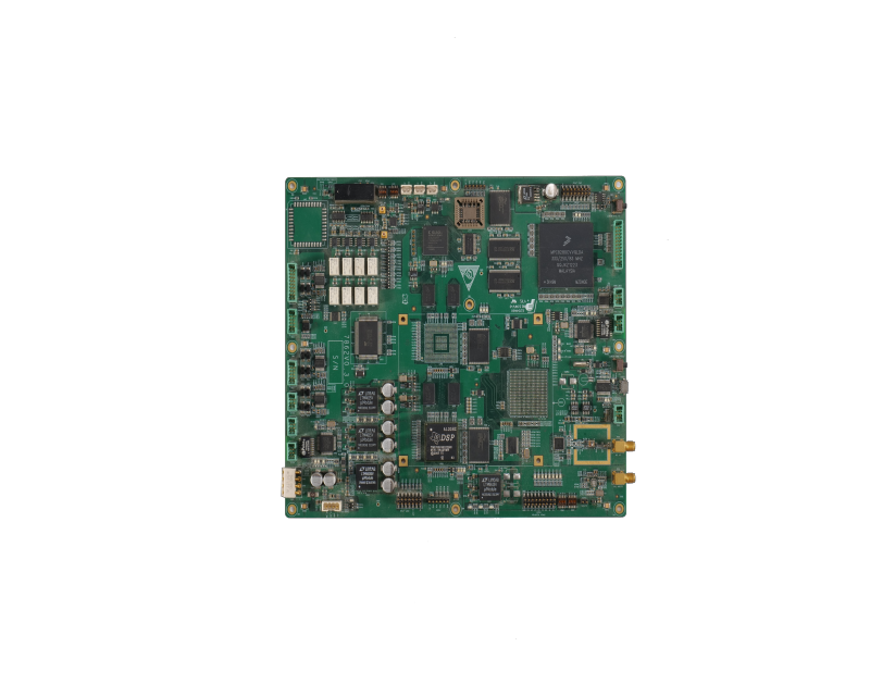
Connections between PCB, circuit diagrams, and electronic components
Planning is the keyword that defines PCB manufacturing, as the entire creation process is orderly. Circuit debugging and troubleshooting are related to the prior logical organization of components. That is to say, before making the circuit, the connection and function of each component in the circuit must be carefully considered, so that it is possible to avoid problems such as poor wiring contact.
Planning is the keyword that defines PCB manufacturing, as the entire creation process is orderly. Circuit debugging and troubleshooting are related to the prior logical organization of components. That is to say, before making the circuit, the connection and function of each component in the circuit must be carefully considered, so that it is possible to avoid problems such as poor wiring contact.
The electrical design of a PCB starts with a schematic diagram (SEF, functional electrical diagram). Whether using Cadence OrCAD or Mentor DxD, electrical designers will begin by studying the electrical functions to be created.
Once all necessary components are identified, a bill of materials (BOM) is created for purchasing. The drawing of the schematic diagram proceeds simultaneously with the BOM; electrical symbols are placed first, then connected via so-called "nets". Once the wiring diagram is finalized, a "netlist" and a table representing the existing electrical connections and components used are exported. Once the netlist is exported, it is imported into the routing software, which translates each line of code into connections corresponding to all existing components indicated.
Placement is one of the key stages of the main PCB, as the choice and placement criteria of components will affect the routing of tracks. Good placement at this stage will avoid many problems with interference, crosstalk, and critical signal coupling. When placing components, the electrical function of the parts is always considered, avoiding placement and routing restrictions. Track routing is the interconnection of all connections between components in the wiring diagram. The tracks to be created will connect the component pads and will use multiple interconnect layers to concentrate all connections within the PCB. The layers are interconnected via metallized holes (also known as vias). The dimensions of the tracks will be calibrated appropriately according to the electrical limitations of the signals passing through the board. All electrical insulation must be carefully selected (track-track, track-spacing, spacing-spacing, track-ground plane, ground plane-via, track-clearance, spacing-clearance, etc.).
Impedance control, crosstalk, and signal integrity
Particular attention should be paid to impedance control and relative adaptation in order to always achieve the conditions for greater power transfer between the generator and the user.
During routing, critical signals must be identified and handled correctly immediately to avoid crosstalk or crosstalk problems, as it is the electromagnetic field generated in the tracks when current flows, producing energy exchange from one track to another.
This can cause undesirable interference due to induced stray currents, affecting signal quality and leading to reduced communication speed.
Good digital signals have fast transitions and clean logic levels without transients.
A schematic diagram is a diagram showing the circuit connections within the component code of a circuit.
A schematic diagram is a diagram showing components and their relationships drawn using physical and electrical standardized symbols, used for research and technical planning.
Schematic diagrams can convey the working principle of components, analyze their performance, and provide a planning system for installing electronic and electrical products.
In circuit design, technicians confirm on paper or computer after the actual installation is completed.
Improvements, repairs, and success are achieved through debugging.
Using circuit simulation software for circuit-aided design and virtual circuit experiments can improve engineers' efficiency, save learning time, and make the real picture more intuitive.
The shape of the parts in the circuit is not necessarily similar or completely different from the actual parts.
But generally represents the characteristics of the component, the number of pins matches the actual component.
Like many wires in radio schematic diagrams, they are not necessarily straight lines in printed circuit board diagrams, but can also be copper films of specific shapes.
A node represents a connection between multiple pins or wires.
All pins and conductors of components connected to a node are conductive, regardless of how many there are.
Annotations are very important in schematic diagrams; all text in a schematic diagram can be classified as annotations.
If you look closely at the diagram above, you will find that various parts of the schematic diagram have annotations. Annotations indicate the type, name, etc., of the components.
PCB drawing software
Since the official birth of commercial CAD systems (EDA), since 1981, various design software has emerged. Printed circuit boards are the backbone of any hardware product. Before the advent of EDA software, engineers typically designed electronic circuits and integrated circuits manually or by other non-automated methods.
STM32WB PCB design characteristics
The microwave traces of the printed circuit board must be carefully designed. Let's consider the main aspects of the PCB design of the STM32WB. Let's start with impedance matching.
As is well known, in order to reduce signal reflections, the impedance of the source, receiver, and transmission line must be matched.
The impedance of the transmission line depends on its geometry and the position of the supporting plane. By reference plane, I mean a conductive layer with zero potential, whose geometric dimensions are significantly larger than those of the conductive lines.
The following lists the main factors affecting the characteristic impedance of a transmission line:
Line type: microstrip line, stripline, coplanar line;
Line width;
Distance to the supporting layer H (dielectric thickness);
Dielectric material parameters (dielectric constant);
The thickness of the conductive layer, which is more significantly affected by the conductor T1 thickness and less by the reference layer T2 copper thickness;
Solder mask thickness;
The impedance of the transmission line depends on its geometry and the chosen PCB layer stackup. There are two design approaches, depending on whether the priority is given to the stackup or the geometry.
One approach is for the circuit board developer to define the conductor geometry convenient for themselves and then select the layer stack and production technology. However, finding the required stack within the technological limitations of the PCB manufacturer is not always possible.
It may happen that even if the manufacturer is able to produce a board with a given stack, its cost will be significantly higher than that of a typical board, especially in small-batch production or prototyping. Another approach is to choose a common stack from the manufacturer.
Each PCB manufacturer has recommended solutions that ensure lower production costs. But in this case, you have to choose the geometry of the transmission line based on the available parameters, which is not always suitable for the developer. Both approaches require close cooperation between the developer and the manufacturer.
Conclusion
This article defines the meaning of PCB and introduces related content, such as PCB function, PCB manufacturing location, and PCB design. To obtain high-quality and reasonably priced PCBs, you can cooperate with a source factory PCB manufacturer, from whom you will receive satisfactory service and products.
RECOMMENDED NEWS

High-end Custom Services: SMT Chip Processing Meets Diverse Industry Needs


(Telephone contact)
Email:
Address: Room 502, Building 1, No. 13, Bohua 4th Road, Huangpu District, Guangzhou City
COPYRIGHT © 2025 Guangzhou Tongsen Electronic Technology Co., Ltd. All rights reserved.