Welcome to Guangzhou Tongsen Electronic Technology Co., LTD. Website!


What is PCBA and how to customize PCB assembly
A PCBA, or Printed Circuit Board Assembly, is a circuit board with surface-mount and/or through-hole mounted electronic components (such as capacitors, resistors, and ICs). Some PCBAs may embed components, such as LTCC ceramic PCBs.
PCBA stands for Printed Circuit Board Assembly, which is an electronic mainboard or module formed by soldering components onto a blank PCB.
It involves using insulating material sheets, copper foil, and solder resist. Once it's soldered with the required components and passes inspection, it becomes a PCBA.
Here are the PCBA details revealed in this article:
Part 1: What is PCBA?
PCBA, or Printed Circuit Board Assembly, refers to a circuit board with surface-mount and/or through-hole mounted electronic components such as capacitors, resistors, and ICs. Some PCBAs can embed components, such as LTCC ceramic PCBs.
A PCBA includes the PCB and the components. The PCB uses conductive traces and pads etched from copper layers laminated between non-conductive sheets. Components are soldered onto the PCB to make electrical and mechanical connections.
To ensure proper connections between the PCB and components, solder needs to be soldered or inserted into the blank circuit board and inspected to test its performance.
In a PCBA, copper wires on different layers are interconnected through plated-through holes, and electronic components are soldered onto the PCB copper pads or inserted through plated-through holes. Additionally, a PCBA can have two component mounting surfaces.
A PCBA is a semi-electrical product suitable for various products, ranging from small LED lights to large industrial control systems. When a PCBA is fitted with a casing and other parts, they become a boxed product or final product.
Part 2: How to Get a Custom PCBA
Step 1. One step to design a custom PCB is to create a schematic.
Place the required components on the canvas and connect their pins with wires representing electrical connections. Components are usually taken from a component library in the design software.
Depending on the package type used (e.g., Dual In-line Package or Surface Mount Chip), the same component may have multiple variants. The packages may look the same in the schematic but very different in the layout view of the board design.
Besides the components and their electrical connections, power and ground signals are also needed. Additionally, connectors must be placed on the PCB to allow space for power and ground. The board also needs connections to external devices such as potentiometers, LEDs, etc.
Step 2. Once everything is ready, an electrical rules check will be performed to ensure there are no obvious faults.
These may include broken wires or connections or any missing ground or power connections, etc. Once the schematic is complete, the board layout view will be checked.
Step 3. Move the components to reasonable and appropriate positions.
Step 4. For board production, signals are assigned to each layer, and different signals on a single layer cannot touch.
Step 5. Once the signal placement is complete, a design rule check needs to be run to ensure the correct placement of holes, traces, etc. These rules can also be customized.
Step 6. If the design is approved, the design files can be uploaded.
The communication language for PCB manufacturing is Gerber files. Each board has multiple files, one for each layer. Another file called the "drill file" defines where holes need to be drilled.
Step 7. Go to the online quoting system and click "Browse Files" to upload the Gerber.
After uploading the Gerber, it will run an error checking program. It will generate an image file of the PCB. You need to input the required number of PCBs.
Step 8. Check the PCB specifications, select the delivery time, and click "Buy Now." Follow the next instructions on the screen.
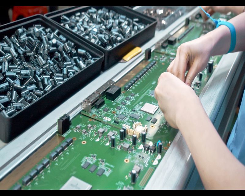
Part 3: PCBA Manufacturing - SMT and PTH
Almost all PCBAs now use Surface Mount Technology, which is automated, while the semi-automated Through-Hole Technology (PTH) is rarely used.
Surface Mount Technology
Surface Mount Technology (SMT) represents the entire technology of soldering components onto the surface of a PCB. In SMT, components or SMDs have no leads or only short leads.
The SMT assembly process is automated and efficient, including solder paste printing on PCB pads, solder paste inspection, SMD placement, reflow soldering, automated optical inspection (AOI), etc.
SMT does not require corresponding holes to be reserved for SMDs, suitable for high-density circuits, smaller SMD packages are 01005. The finer pitch (distance between the centers of adjacent SMDs) is 0.05mm.
Through-hole PCB assembly (PTH) refers to soldering component leads into through-holes on the PCB board. THT is usually divided into single-ended, double-ended, pin grid array, etc.
Usually, the leads of electronic components are manually inserted into pre-set holes on the PCB board, the PCBA is placed in a jig that only exposes the area that needs wave soldering and preheated, then put into a wave soldering furnace to solder the THT component leads and through-holes.
For large-scale PCBA manufacturing, SMT is more efficient and economical than THT.

Part 4: PCBA Inspection
Various inspections are needed throughout the PCB assembly process to ensure robust connections and functionality of the PCBA.
During the PCB assembly process, PCBA inspections are performed in the following chronological order:
Solder Paste Inspection (SPI): After screen printing solder paste on the PCB, it will go through an SPI machine. An infrared camera scans the solder paste, and a computer compares the specifications with pre-entered standard specifications to ensure that the size, thickness, and position of the solder paste are suitable for soldering. Only after this inspection can the PCB proceed to the step of placing surface mount devices (SMDs).
X-ray Inspection of BGAs: If the SMDs include Ball Grid Arrays (BGAs), the PCBA should go through X-ray inspection before reflow soldering. This inspection ensures that the solder balls of the BGA are intact and suitable for soldering.
Visual Inspection: Before reflow soldering, every effort should be made to ensure foolproof. Therefore, there is a Quality Control (QC) team on the SMT production line to inspect the surface of the PCBA.
Automated Optical Inspection (AOI): After reflow soldering, each PCBA must pass through an AOI machine to ensure there are no soldering errors, including solder bridges, component offsets, solder voids, tombstones, etc.
Secondary Visual Inspection: After AOI, the QC team needs to inspect the PCBAs to ensure that no component or board aging has occurred due to excessive reflow.
First Article Inspection (FAI): During the PCBA prototyping phase, we manufacture 5 pieces, and randomly select 1 PCBA for FAI. Professional technicians use a probe pen connected to the FAI machine to contact each PCBA component. The values of the PCBA components are recorded and compared with the pre-entered values. After FAI is completed, a report will be automatically generated. We will send it to the customer for review. Only after customer approval can we begin mass PCB assembly.
Two Additional Visual Inspections: Before and after wave soldering, our QC technicians visually inspect the PCBAs to ensure there are no problems.
PCBA Multimeter Inspection
Multimeter Inspection: During the PCB design phase, you need to use a multimeter to design test pads for key components on the PCBA. After PCB assembly, we will use the two probes of the multimeter to contact the test pads to ensure the key components on the PCBA are functional. This is a necessary PCBA inspection.
Functional Test: After PCB assembly, there is also a functional test for the PCBA, which is an optional inspection. The PCBA is placed on a fixture that is powered on and connected to a computer. The computer will display the PCBA's pass/fail result on the screen.
Thermal Aging: Thermal aging is a PCBA inspection that checks whether the PCBA can function normally after prolonged continuous operation. Depending on application requirements, the aging time varies from 12 hours to 168 hours.
Simulation Test: After installing the casing, the PCBA is a complete machine or final product. To ensure that the complete machine works as expected, we can simulate the application field before delivery to view the product's operating results.
In addition, for flexible PCBs, PCBA inspection also includes tensile testing, bending testing, sweat testing, environmental testing, metallographic inspection, bridging testing, pressure resistance testing, impedance testing, etc.
RECOMMENDED NEWS

High-end Custom Services: SMT Chip Processing Meets Diverse Industry Needs


(Telephone contact)
Email:
Address: Room 502, Building 1, No. 13, Bohua 4th Road, Huangpu District, Guangzhou City
COPYRIGHT © 2025 Guangzhou Tongsen Electronic Technology Co., Ltd. All rights reserved.