Welcome to Guangzhou Tongsen Electronic Technology Co., LTD. Website!


How to avoid short circuits in SMT chip processing? What are the causes of IC short circuits (bridging)?
Short circuits during SMT processing frequently occur between the pins of fine-pitch ICs, hence the term "bridging." While short circuits can also occur between chips, this is rare. Below is a brief discussion of the causes and solutions for bridging between the pins of fine-pitch ICs.
SMT processing short circuits. This type of defect frequently occurs between the pins of fine-pitch ICs, so it is also called "bridging." Of course, there are also short circuit phenomena between CHIP components, but this is rare. Below, we will briefly discuss the causes and solutions of bridging problems between the pins of fine-pitch ICs.
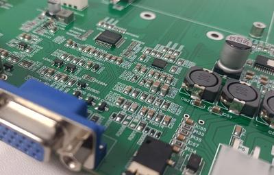
Bridging phenomena frequently occur between IC pins with a spacing of 0.5mm or less. Because the spacing is small, even slight flaws in the stencil design or printing can easily lead to this problem.
I. Stencil
According to the IPC-7525 stencil design guidelines, to ensure that the solder paste can be smoothly released from the stencil openings to the PCB pads, three factors are mainly relied upon in terms of stencil openings:
1. Area ratio/width-thickness ratio > 0.66
2. Smooth stencil hole walls. Electropolishing is required during the manufacturing process.
3. With the printing surface facing upwards, the lower opening of the stencil hole should be 0.01mm or 0.02mm wider than the upper opening, forming an inverted cone shape, to facilitate effective solder paste release and reduce the frequency of stencil cleaning.
Specifically, for ICs with a spacing of 0.5mm or less, due to their small pitch, bridging is easily produced. The length of the stencil opening remains unchanged, while the width is 0.5~0.75 times the pad width. The thickness is 0.12~0.15mm. Laser cutting and polishing are preferred to ensure that the opening is trapezoidal and the inner walls are smooth, facilitating good solder flow and shaping during printing.
II. Solder Paste
The correct choice of solder paste is also crucial in solving bridging problems. For ICs with a spacing of 0.5mm or less, solder paste with a particle size of 20~45um and a viscosity of around 800~1200pa.s should be selected. The solder paste activity can be determined based on the cleanliness of the PCB surface; RMA grade is generally used.
III. Printing
Printing is also a very important step.
1. Squeegee type: There are two types of squeegees: plastic and steel. For ICs with PITCH ≤ 0.5mm, a steel squeegee should be used during printing to facilitate the shaping of the solder paste after printing.
2. Squeegee adjustment: Printing at a 45° angle can significantly improve the imbalance of solder paste on different stencil opening directions and reduce damage to fine-pitch stencil openings; the squeegee pressure is generally 30N/mm2.
3. Printing speed: Under the push of the squeegee, the solder paste will roll forward on the stencil. A faster printing speed is beneficial for stencil rebound but will hinder solder paste leakage; if the speed is too slow, the solder paste will not roll on the stencil, resulting in poor resolution of the solder paste printed on the pads. Typically, the printing speed range for fine-pitch is 10~20mm/s.
4. Printing method: Currently, the most common printing methods are "contact printing" and "non-contact printing." Printing methods with a gap between the stencil and the PCB are called "non-contact printing." The gap is generally 0.5~1.0mm. The advantage is that it is suitable for solder pastes with different viscosities. The solder paste is pushed into the stencil opening and into contact with the PCB pads by the squeegee. After the squeegee is slowly moved away, the stencil will automatically separate from the PCB, reducing the trouble of stencil contamination caused by vacuum leakage.
Printing methods without a gap between the stencil and the PCB are called "contact printing." It requires the stability of the overall structure and is suitable for printing high-precision solder paste. The stencil and PCB maintain very flat contact and separate from the PCB only after printing. Therefore, this method achieves higher printing accuracy, especially suitable for fine-pitch and ultra-fine-pitch solder paste printing.
IV. Mounting Height
For ICs with PITCH ≤ 0.5mm, a mounting height of 0mm or 0~-0.1mm should be used during mounting to avoid solder paste collapse due to excessively low mounting height, causing short circuits during reflow.
V. Reflow
1. Too fast heating rate 2. Too high heating temperature 3. Solder paste heats up faster than the circuit board 4. Too fast flux wetting speed.
RECOMMENDED NEWS

High-end Custom Services: SMT Chip Processing Meets Diverse Industry Needs


(Telephone contact)
Email:
Address: Room 502, Building 1, No. 13, Bohua 4th Road, Huangpu District, Guangzhou City
COPYRIGHT © 2025 Guangzhou Tongsen Electronic Technology Co., Ltd. All rights reserved.