Welcome to Guangzhou Tongsen Electronic Technology Co., LTD. Website!


A Step-by-Step Guide to Printed Circuit Board Assembly (PCBA) Process (Part 1)
The temperature rapidly rises above the solder paste melting point (typically 183 – 220°C). The solder paste melts, dissolving the PCB pad metallization layer and component leads to form solder joints, which then cool and solidify.
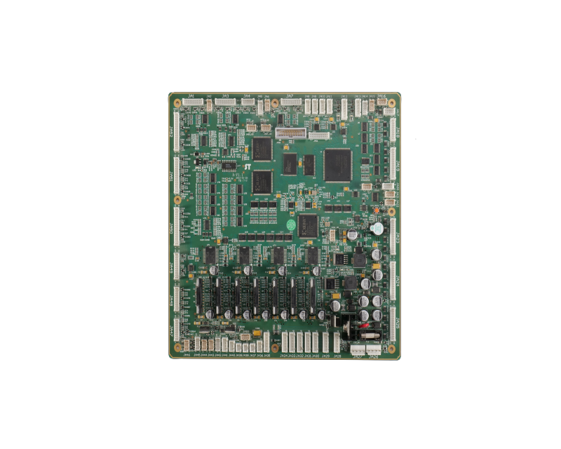
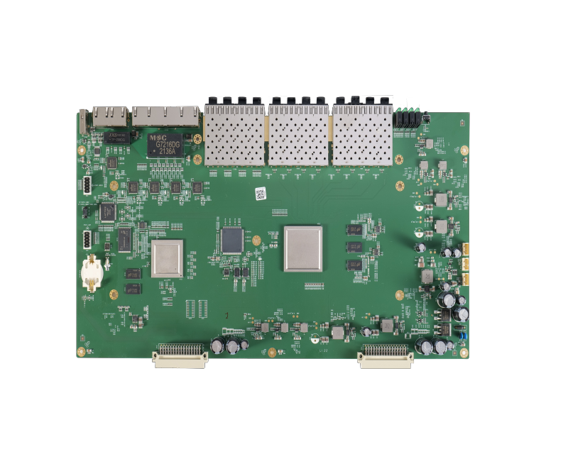
Printed Circuit Board Assembly (PCBA) is the process of soldering or assembling electronic components onto a PCB, or printed circuit board. It involves mounting and soldering components such as capacitors, resistors, integrated circuits (ICs), transistors, and other parts onto the PCB. The completed PCB assembly is a major component of electronic devices and equipment.
The PCBA process is complex and precise, requiring expertise, training, and the right tools and equipment. This step-by-step guide will walk you through the typical stages and key steps involved in assembling a PCB from start to finish.
PCBA Process Overview
A typical PCBA process includes the following key stages:
1. Solder Paste Printing
2. Component Placement
3. Reflow Soldering
4. Inspection and Testing
5. Repair and Rework
6. Conformal Coating
7. Final Testing and Quality Inspection
This manufacturing stage sequence enables efficient, high-quality PCB component assembly. The following sections will describe these PCBA process stages in more detail.
Stage One: Solder Paste Printing
Solder paste printing is a step in the PCBA process. It involves applying a controlled amount of solder paste to the PCB pads and connecting pads.
Some key steps in solder paste printing include:
PCB Preparation — Cleaning, pre-baking the bare PCB, and preparing it for solder paste printing.
Stencil Alignment — The solder stencil is carefully aligned on the PCB to ensure accurate solder paste transfer.
Solder Paste Dispensing — Solder paste is dispensed onto the stencil surface, typically using an automated solder paste printer. The solder paste is usually an alloy of tin and lead.
Solder Paste Transfer — The solder stencil is lowered and pressed onto the PCB surface to transfer the solder paste to the pads.
Stencil Cleaning — After printing, the stencil is thoroughly cleaned to remove any residual solder paste.
PCB Inspection — The PCB solder paste deposits are inspected under a microscope or an AOI (Automated Optical Inspection) machine.
Stage Two: Component Placement
Component placement is the process of mounting various electronic components onto their designated locations on the PCB and applying solder paste. Steps include:
Bill of Materials (BOM) — The types and quantities of components required for PCB assembly are detailed in the BOM document.
Component Preparation — Preparing components according to specifications — straightening, forming, cutting, etc.
PCB Fixture — The circuit board is correctly secured in place on a conveyor platform.
Automated/Manual Placement — Components are accurately placed onto the correct polarity pads either manually or via an automated pick-and-place machine.
Glue Dispensing — Some components (e.g., large connectors) are secured to the PCB with glue before soldering.
Key factors to consider when placing components:
Component Profile — Shape, size, lead spacing
Pad Size, Location — Component pad alignment
Polarity — Placing the component in the correct orientation
Population Sequence — Components from smallest to largest
While manual placement requires human operation, automated pick-and-place systems are ideal for fast, high-volume PCB assembly. They can place 25,000-50,000 components per hour.
Stage Three: Reflow Soldering
Reflow soldering is the process of creating reliable electrical and mechanical joints between components and the PCB board by controlled heating and melting of the solder. Stages in the reflow process include:
a. Preheat
The PCB assembly is slowly preheated to approximately 150°C to evaporate volatile flux components and prevent thermal shock to the components.
b. Soak
The temperature is held between 150-200°C for approximately 60-120 seconds. This ensures even heating of the board and components.
c. Reflow
The temperature is rapidly increased to above the solder paste melting point (typically 183 – 220°C). The solder paste melts, dissolving the PCB pad metallization and component leads, forming solder joints, which then cool and solidify.
Reflow cycle parameters (including time and temperature ranges) for each zone are carefully optimized depending on the solder alloy used. Common reflow soldering methods include:
Infrared Reflow — Infrared radiant heaters and convection fans are used to heat and reflow the solder joints.
Vapor Phase Reflow — Condensation of a vaporized inert liquid provides rapid, uniform heating for reflow.
Laser Reflow — A computer-controlled laser beam selectively preheats and activates the solder paste.
Wave Soldering — The bottom side of the PCB contacts a wave of flowing molten solder. Less commonly used now.
RECOMMENDED NEWS

High-end Custom Services: SMT Chip Processing Meets Diverse Industry Needs


(Telephone contact)
Email:
Address: Room 502, Building 1, No. 13, Bohua 4th Road, Huangpu District, Guangzhou City
COPYRIGHT © 2025 Guangzhou Tongsen Electronic Technology Co., Ltd. All rights reserved.