Welcome to Guangzhou Tongsen Electronic Technology Co., LTD. Website!


How to make a PCB?
Now that we understand what PCBs are and the related terminology, why not learn how they are manufactured? It's a somewhat complex process, but don't worry! Here you can find a step-by-step procedure for PCB production.
Now that we understand what PCBs are and the related terminology, why not learn how they are manufactured? It's a somewhat complex process, but don't worry! Here you can find a step-by-step procedure for PCB production.
The designer will first prepare the PCB layout on a Computer-Aided Design or CAD system. There are various software packages available for this purpose, but we prefer and recommend using KiCad. The PCB design will be saved in Gerber format, which is the de facto standard. Gerber files contain a 3D model of the PCB and define the copper foil, solder mask, and silkscreen layers.
Simultaneously, copper foil is laminated onto the substrate's flat plate. A protective aluminum is then applied. This layer is then aligned and sent for drilling according to the pre-prepared Gerber files. Positioning holes are drilled first. Afterward, the machine will drill holes for each PCB on the panel to secure components to the board. Mounting holes for each PCB will also be drilled. After drilling, the circuit boards are thoroughly cleaned to remove any residue.
The next and important step is the creation of the copper traces. This is achieved through a chemical process called etching. The copper foil is covered with a resist mask, the pattern of which is the same as the circuit we want the PCB to have. Then, the unnecessary copper, or copper that will not be part of the circuit, is removed. This can be done with an alkaline or acidic solution. In this example, we will use an alkaline solution. The entire layer with the resist mask is immersed in an alkaline solution of 60 to 120 degrees Celsius (140 to 248 degrees Fahrenheit). The areas not covered by the resist mask will dissolve. Once completed, the resist mask is rinsed away to reveal the desired copper traces.
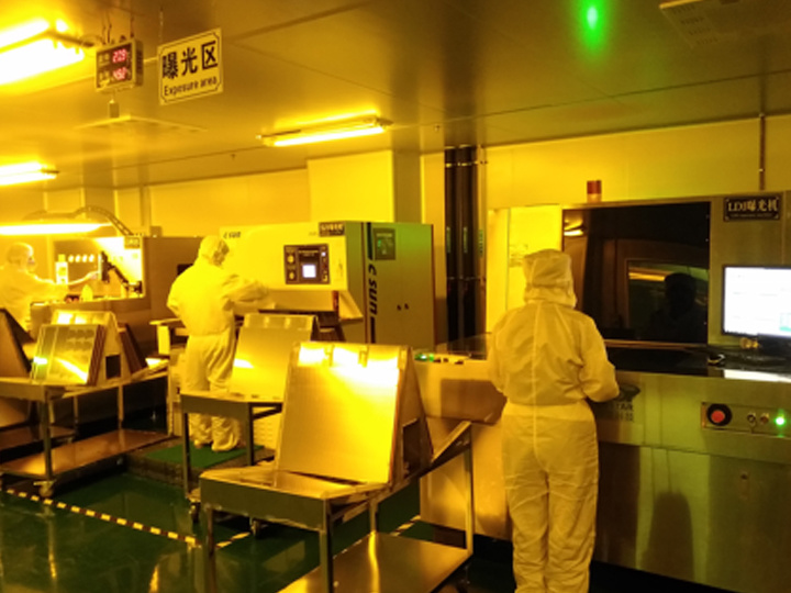
The board is then sent for inspection to check its quality. Since the copper traces are very fine, the operator will use an optical inspection machine to check the board. They do this by taking pictures of the copper traces and comparing them to the PCB design file. If the board has any broken or shorted traces, it is discarded. If everything is fine, the board proceeds to the next step - solder mask application.
The insulating solder mask protects the board from exposure to dust and oxidizing environments. The copper traces are hidden under the colored solder mask. If not careful, the solder mask will block the conductive vias needed to connect components correctly. This can be easily avoided. First, the edge area of the holes is covered with a chemically resistant solder mask. Then, the solder mask is applied to the entire PCB. Then, the board is UV-treated, removing the chemically resistant solder mask and solder mask from the edges. This way, the edge area of the holes is exposed - now only the desired conductive copper remains.
Silkscreen printing. It's just a layer of ink used to identify PCB components, symbols, markings, logos, etc. Besides providing information, it doesn't offer any other functionality.
The PCB is now complete. What was initially a simple copper plate is now a fully functional circuit board. Now, you can solder components using liquid tin or ship the bare board to suppliers and companies.
Assembling the PCB
After making the PCB, let's see how to assemble it into a functional board. To assemble a PCB, you will almost always use some SMD components. Compared to THT components, they allow for lower costs and higher quality of the final product.
Unlike THT, SMD components do not require drilling holes in the circuit board. They will be placed on the pads. There are two ways to apply solder paste to the pads on the PCB. One method is to use a laser-cut stainless steel or nickel stencil. The stencil with the pad pattern and locations is placed on top of the panel. Then, the solder paste is poured into it. A specialized squeegee is used to evenly distribute the solder paste across the circuit board. Another way to add solder paste to the PCB is to use an inkjet printer. This is very similar to how an inkjet printer works.
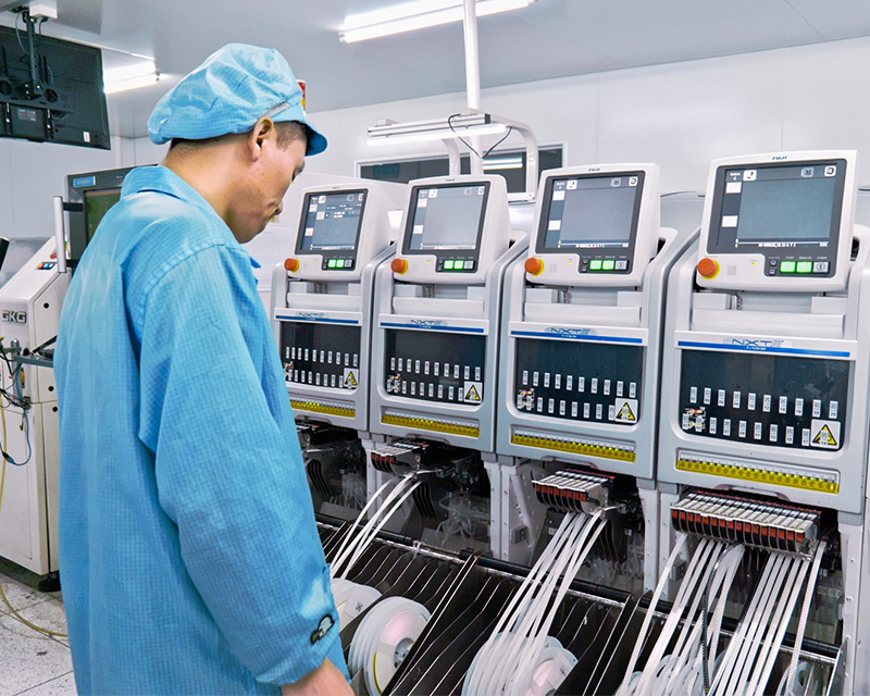
After adding the solder paste, the board is placed on the conveyor belt of the pick-and-place machine. The components are placed on reels or plastic tubes in the machine. The machine's camera will first determine the coordinates of the reference points on the panel to locate the PCB's pads. Using a pre-written program, the machine will pick up components from the reels or plastic tubes and place them on the panel according to the PCB design document. A wide variety of components are placed this way, from large chips to small LEDs.
Then, the PCB with the components mounted moves along the conveyor belt directly into the reflow oven. The oven has several zones, each with a different temperature. The board enters a preheating zone and then passes through zones of gradually increasing temperature. This is to prevent thermal shock. Once the board enters a zone of sufficiently high temperature, the solder paste melts, bonding the component leads to the pads on the PCB. The surface tension of the molten solder will hold the components in place and align them as the solder cools. After soldering, while the board is still slightly cooling, it is cleaned to remove any possible residue.
Next, a visual inspection of the board is performed to check for missing components or incorrect soldering. This can be done by an Automated Optical Inspection system. The machine can control many factors such as missing components, deviations in component placement, polarity, etc. Boards with detected defects are sent to a rework station where any errors are manually repaired by hand.
After assembling the SMD components, the THT components are mounted. There are two ways to achieve this: wave soldering and selective soldering. In wave soldering, the PCB passes over a wave of molten solder, the solder is pumped so it looks like a standing wave. As the board contacts this wave of solder, the components are soldered to the board. This is a good way to solder a large number of components in a short time. The other method is selective soldering. Here, individual through-hole components are soldered one by one. A fountain of molten solder moves to the position below the circuit board, soldering the components from below. This process is not only faster and repeatable compared to manual soldering, but also results in better results and fewer errors.
When all components are mounted on the board, the electronic module will go through a final quality control step. Visual quality control will be performed using inspection equipment before the product is packaged and sent to the customer.
How to design your PCB
Have you ever thought about making your own PCB but weren't sure if you could do it? We are living proof that it's entirely possible! We could go into all the details, but we prefer to be brief and informative. That's why we've listed 6 quick tips before you begin.
You need to understand the electrical parameters. There's no way around this. These are fundamental before making a PCB. Current ratings, voltage, signal types, impedance, capacitance, etc., are all terms you should understand before making and assembling a PCB.
Choose your CAD system. There are free and paid options available. We used it when we started making PCBs, and we still use it professionally today! Look for a CAD with a good community and is (relatively) easy to use. No community means you'll get almost no help if you run into trouble, and complex software will only frustrate you and make you give up quickly.
Don't copy other people's work. Thanks to open-source hardware, this is easier than ever. But don't steal! There are plenty of layouts available, so you can see how others have done it before you. Use them as inspiration or learning material, but never claim them as your own! It's unethical and could get you into a lot of trouble.
Schematics are crucial. Good schematics make good circuit boards. When making PCBs, it's best to start with a schematic. A schematic is basically like a blueprint for a new device. They show which components are used in the design, how they are connected, and the relationships between groups of components in different schematic sheets.
Communicate component placement. If you are designing a PCB and sourcing from external suppliers, you will likely discuss its layout and design. Good communication is key. There may be some standards and rules as to why certain components cannot be used together. This is because they may create electrical noise in the circuit when they are close to each other. The PCB supplier will provide datasheets for each component, so you will have all the necessary information.
Practice a lot and don't get discouraged. Designing PCBs may seem complicated at first glance, and it is! But that doesn't mean you shouldn't do it. Quite the opposite! Your first circuit board design will likely have many problems. Your next design will have fewer problems. As long as you keep learning, you will improve over time. We still sometimes have problems when designing circuit boards, and we've been doing this for many years. So don't fret over mistakes. After all, that's how we learn!
When you learn how to make PCBs, you may find it very worthwhile. If you are making multiple projects, you can easily adjust the PCB design to your needs. This is much better than using a pre-made circuit board and adjusting your project around it.
RECOMMENDED NEWS

High-end Custom Services: SMT Chip Processing Meets Diverse Industry Needs


(Telephone contact)
Email:
Address: Room 502, Building 1, No. 13, Bohua 4th Road, Huangpu District, Guangzhou City
COPYRIGHT © 2025 Guangzhou Tongsen Electronic Technology Co., Ltd. All rights reserved.