Welcome to Guangzhou Tongsen Electronic Technology Co., LTD. Website!


Causes and preventive measures for SMT surface mount soldering defects
The above content is about the causes and preventive measures of SMT surface mount soldering defects. I believe you have already understood it. Because the SMT surface mount soldering process is complicated, some soldering problems are unavoidable in the work. We should learn to analyze the causes of each problem and seek solutions, focusing on prevention and reducing soldering defects.
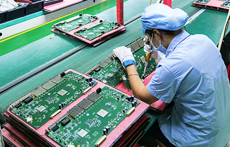
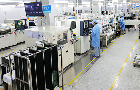
With the development of SMT surface mount technology, the requirements for SMT processing technology are becoming increasingly higher. SMT soldering is closely related to all aspects of the entire assembly process. Once soldering problems occur, they will affect product quality and cause losses.
1. Bridging
Bridging refers to the solder incorrectly connecting two or more adjacent pads, causing electrical contact and forming a conductive path. The causes of bridging are often excessive solder or severe solder collapse after solder printing, or misalignment of the substrate welding area size, SMD mounting offset, etc. In the stage where SOP and QFP circuits are becoming more miniaturized and refined, bridging can cause electrical short circuits and affect product use.
Preventive measures:
1. Set the size of the substrate welding area and the SMD installation position according to the design requirements.
2. To prevent poor edges during solder paste printing, the gap between the substrate wiring and the accuracy of the solder resist coating must meet the requirements.
3. Formulate appropriate welding process parameters to prevent mechanical vibrations of the welding machine conveyor belt.
Solder balls
Solder balls refer to scattered solder balls formed in unnecessary locations on the circuit board due to solder splashing during the soldering process. The generation of solder balls is mostly due to rapid heating and solder splashing during the welding process. In addition, it is also related to solder paste printing misalignment, edge collapse, and contamination.
Preventive measures:
1. Implement the corresponding preheating process according to the welding type.
2. Perform welding according to the set temperature process to avoid excessive heating during welding causing defects.
3. The solder paste used should meet the requirements and have no problems such as poor hygroscopicity.
Cracks
When the printed circuit board is just separated from the welding area during welding, due to the difference in thermal expansion between the solder and the connected part, under the action of rapid cooling or rapid heating, the SMD will produce microcracks due to the influence of solidification stress or shrinkage stress. The welded PCB must also reduce the impact stress and bending stress on the SMD during stamping and transportation.
Preventive measures:
1. When designing surface mount products, the gap of thermal expansion must be considered, and the heating and cooling conditions must be set correctly.
2. Select solder with good ductility.
Pull-up tip
Solder bridging refers to the appearance of sharp tips or burrs at the solder joint. The reasons are excessive solder, insufficient flux, excessive heating time, excessive welding time, and improper soldering iron pulling angle.
Preventive measures:
1. Select the appropriate flux and control the amount of solder.
2. Set the preheating temperature according to the PCB size, whether it is a multilayer board, the number of components, and whether there are mounted components.
Vertical film problem (Manhattan phenomenon)
The Manhattan phenomenon refers to the phenomenon where one end of a rectangular surface mount component is welded to the pad, while the other end is tilted. The main reasons for this phenomenon are uneven heating of both ends of the component, unbalanced heating direction, solder paste melting and welding area size, SMD shape itself, wettability, etc.
Preventive measures:
1. Adopt a reasonable preheating method to achieve uniform heating during welding.
2. Reduce the surface tension of the SMD end when the solder melts.
3. The length of the substrate welding area should be appropriately set, and the printing thickness of the solder should be correctly set.
Poor wettability
Poor wettability refers to the failure of the solder to react with the substrate welding area during the welding process after wetting, resulting in missing solder or insufficient solder. The reasons are mostly due to contamination of the welding area surface, or due to solder resistance, or due to the formation of a metal compound layer on the joint surface.
Preventive measures
1. In addition to implementing appropriate welding processes, anti-fouling measures should also be taken on the surface of the substrate and components.
2. Select the appropriate solder and set reasonable welding temperature and time.
The above is the reason and preventive measures for poor welding in SMT surface mount processing. I believe everyone has a certain understanding. Because the SMT welding work in the SMT surface mount processing process is relatively complex, some welding problems are unavoidable in the work. We must learn to analyze the causes of each problem and seek solutions, focusing on prevention and reducing welding defects.
RECOMMENDED NEWS

High-end Custom Services: SMT Chip Processing Meets Diverse Industry Needs


(Telephone contact)
Email:
Address: Room 502, Building 1, No. 13, Bohua 4th Road, Huangpu District, Guangzhou City
COPYRIGHT © 2025 Guangzhou Tongsen Electronic Technology Co., Ltd. All rights reserved.