Welcome to Guangzhou Tongsen Electronic Technology Co., LTD. Website!


Key questions and answers about PCBA
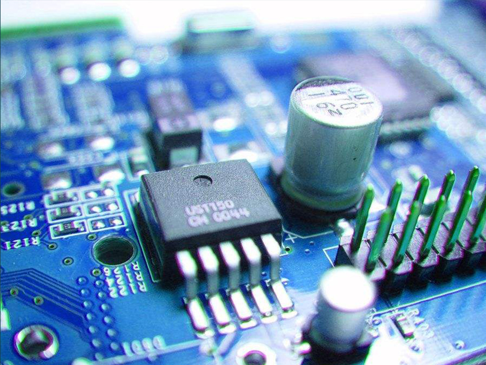
PCB assembly is a complex multi-stage manufacturing process that requires systematic control of materials, machinery, software, and human factors to produce high-quality, fully functional circuit boards. Collaborating with reliable suppliers and automating key processes significantly improves productivity and minimizes errors.
Q1. What are the benefits of solder mask in the PCBA process?
The solder mask offers the following advantages during PCB assembly:
Prevents solder bridging between pads - acts as insulation between closely spaced solder joints.
Protects PCB traces from environmental damage.
Improves solder paste release – makes it easier to remove excess paste after printing.
Aesthetics – gives the assembled board a clean, professional look.
Provides good contrast to aid automated optical inspection.
Allows solder to flow only in the designated pad areas during reflow.

Q2. How to select the right solder paste for PCBA applications?
Key criteria for selecting the correct solder paste are:
Alloy composition (SnPb, SAC, SnAg) depends on the desired solder joint properties and operating temperature.
Particle size distribution – use type 3, 4, and 5 powders for fine-pitch components.
Flux content – use rosin (RA, RMA) or no-clean (RE, NC) flux chemistry depending on residue cleaning requirements.
Printing transfer efficiency based on stencil and printer capabilities.
Shelf life and storage conditions, such as refrigeration requirements.
Reliable supplier with consistent quality and technical support.
Compatible with PCBA production volume. Higher production volume usually means higher solder paste price.
Q3. What are some good practices for component handling in SMT assembly?
Some recommended component handling guidelines are:
Use trays and tapes to transport and store components according to JEDEC standards.
Use a dry cabinet or nitrogen storage to prevent components from absorbing moisture.
Carefully cut component tapes at the designated spacing, avoiding interference with the positioning pockets.
Handle components using vacuum tweezers and avoid mechanical damage.
Set the pressure/vacuum of feeders and placement nozzles according to the mechanical sensitivity of the components.
Visually inspect components and discontinue using the tape if components are detached.
Match the component tape feed rate to the placement capacity of the pick-and-place machine.
Ensure smooth component reel unwinding and tape peeling without jamming.
Regularly maintain, clean, and calibrate feeders to ensure reliable operation.
Q4. What are the main advantages of Automated Optical Inspection (AOI) in PCBA?
Some key advantages of using AOI machines are:
High-resolution cameras can detect minute soldering and component defects.
Can scan both the top and bottom sides of PCB components.
Fast image processing allows for 100% board inspection.
Results are more consistent than manual visual inspection.
Can be integrated with rework workflows for quick turnaround.
Bare board alignment and solder paste inspection can be performed before SMT assembly.
Provides digital records and statistics for all boards for traceability.
Eliminates operator fatigue associated with prolonged manual inspection.
Q5. What defects does ICT testing primarily detect?
Typical defects screened during In-Circuit Test (ICT) include:
Short circuits
Open or lifted traces
Incorrect component values
Poor solder joints
Missing components
Reverse polarity
Board damage or cracks
ICT testers use test probes, fixtures, and appropriate algorithms to uncover manufacturing defects and avoid shipping defective boards to customers.
PCB assembly is a complex multi-stage manufacturing process that requires systematic control of materials, machines, software, and human factors to produce high-quality, fully functional circuit boards. Partnering with reliable suppliers and implementing automation of key processes significantly improves productivity and minimizes errors. Current trends toward smaller, higher-density components and broader process capabilities demand continuous innovation in PCBA processes. By focusing on the details of process design and control, electronics manufacturers can reap the benefits of efficient, low-cost, automated printed circuit board assembly.
RECOMMENDED NEWS

High-end Custom Services: SMT Chip Processing Meets Diverse Industry Needs


(Telephone contact)
Email:
Address: Room 502, Building 1, No. 13, Bohua 4th Road, Huangpu District, Guangzhou City
COPYRIGHT © 2025 Guangzhou Tongsen Electronic Technology Co., Ltd. All rights reserved.