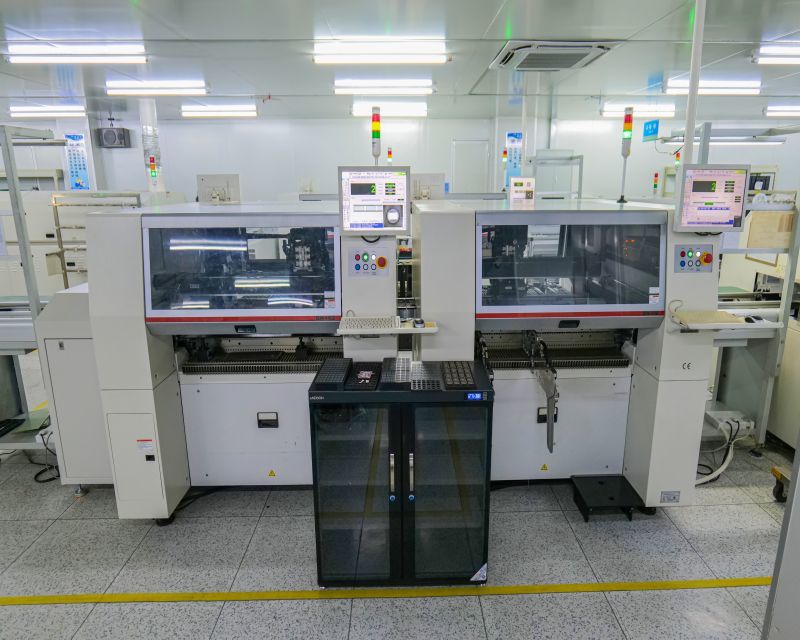
Welcome to Guangzhou Tongsen Electronic Technology Co., LTD. Website!
How to reduce stray capacitance in PCB layout
Effective management of stray capacitance is crucial for achieving high-performance and reliable PCB designs, especially in complex high-frequency and precision analog applications. By leveraging advanced PCB design software, designers can utilize powerful tools for layout, simulation, and analysis to ensure their circuits are optimized for minimal stray capacitance and unimpaired signal integrity.
Stray capacitance in PCB layouts can degrade signal integrity and performance, especially in high-frequency and precision analog circuits. Therefore, understanding and minimizing stray capacitance is crucial for designers aiming to optimize PCBs for superior performance, ensuring the device operates reliably and meets expected specifications.
What is stray capacitance in a PCB?
Stray capacitance in PCB layouts refers to the unintended capacitive effects occurring between conductive components on the board (e.g., between traces, components, and ground planes). This phenomenon is particularly troublesome in high-frequency and precision analog circuits, leading to signal distortion, noise introduction, and an overall decrease in circuit performance. Major contributing factors to stray capacitance include the layout and proximity of conductive components, the dielectric properties of the PCB material, and the arrangement of components and ground planes, all of which can inadvertently promote capacitive coupling between circuit elements.
How to calculate PCB stray capacitance?
The fundamental principle of capacitance is derived from the formula C = Q/V, where C is capacitance, Q is the stored charge, and V is the voltage across the capacitor. This equation highlights the core function of a capacitor: storing charge at a specific voltage. In PCB design, stray capacitance is unintentionally created due to the layout and proximity of conductive elements, acting like tiny, unwanted capacitors distributed across the board.

The specific formula C=ϵA/D details how capacitance in a PCB (or any capacitor) depends on the physical characteristics and materials of the system.
C is the capacitance, measured in Farads (F).
ε (epsilon) represents the dielectric constant of the dielectric material between the conductors.
A is the overlapping area between the conductive elements, measured in square meters (m²).
D is the distance between the conductive elements, measured in meters (m).
This relationship means capacitance increases with increasing overlapping area between conductors and increasing dielectric constant, but decreases with increasing distance between conductors. In PCB design, adjusting these variables helps manage and minimize stray capacitance. For example, increasing the distance between traces or using materials with a lower relative dielectric constant can reduce unwanted capacitive effects.
How to reduce stray capacitance in PCB design?
Reducing stray capacitance in PCB design requires a combination of layout techniques, component placement strategies, and careful material selection. Here are key strategies to minimize stray capacitance, enhance circuit performance, and ensure signal integrity:
1. Increase the distance between conductors
Increase the spacing between traces, pads, and components to reduce capacitive coupling. The capacitance between two conductors is inversely proportional to the distance between them.
2. Optimize trace geometry
Optimizing trace geometry is a crucial strategy in PCB design to reduce stray capacitance, which can adversely affect signal integrity, especially in high-frequency circuits. This optimization involves two primary approaches: reducing trace width and minimizing trace length.
Reduce trace width: For high-frequency signals, use narrower traces to reduce the area facing adjacent traces or planes, thereby reducing capacitance.
Minimize trace length: Shorter traces have a smaller capacitive coupling area, resulting in reduced overall stray capacitance.
3. Use shielding techniques
Employing shielding techniques in PCB design is an effective method for reducing stray capacitance and protecting sensitive circuits from interference. These techniques include the strategic placement of ground planes and the use of guard traces.
Ground planes: Implement effective ground planes to shield sensitive traces from potential capacitive coupling with other signals.
Guard traces: Place grounded guard traces next to high-impedance or sensitive signal lines to mitigate capacitive coupling.
4. Strategic stackup configuration
Design the layer stackup to place ground planes near signal layers, which helps shield and reduce the effective area for capacitance formation. Use pre-planning tools and simulations to optimize the stackup for minimal stray capacitance.
5. Minimize parallelism
Long parallel traces increase capacitive coupling. Avoid parallel routing of sensitive or high-speed traces, especially long runs, when designing the layout.
6. Impedance matching
Proper impedance matching on the PCB reduces reflections and the need for long traces, indirectly helping to minimize stray capacitance. Use impedance calculators and simulation tools to design your traces and corresponding stackup.

Employ specialized routing techniques
For high-frequency circuits, consider using microstrip or stripline configurations, which can help control impedance and stray capacitance through their geometric configuration.
By integrating these strategies into the PCB design process, designers can significantly reduce stray capacitance, ensuring the final product meets the required performance and reliability specifications.
Difference between stray capacitance and parasitic capacitance
Stray capacitance refers to the unintended capacitance that exists between any two conductive parts in a circuit that are separated by an insulating material. This can include capacitance between traces, leads, components, or between traces and ground planes.
Parasitic capacitance is a broader term encompassing all types of unintended capacitance in a circuit, including stray capacitance. It refers to capacitance that is parasitic to the intended circuit elements and degrades circuit performance.
Key Differences
Scope: Stray capacitance is a type of parasitic capacitance, primarily referring to unintended capacitance caused by circuit layout and physical configuration. Parasitic capacitance has a broader definition, including all unintended capacitance affecting circuit performance.
Conclusion
Effective management of stray capacitance is crucial for achieving high-performance and reliable PCB designs, especially in complex high-frequency and precision analog applications. By leveraging advanced PCB design software, designers can utilize powerful tools for layout, simulation, and analysis, ensuring their circuits are optimized for minimal stray capacitance and unimpaired signal integrity.
RECOMMENDED NEWS
High-end Custom Services: SMT Chip Processing Meets Diverse Industry Needs


