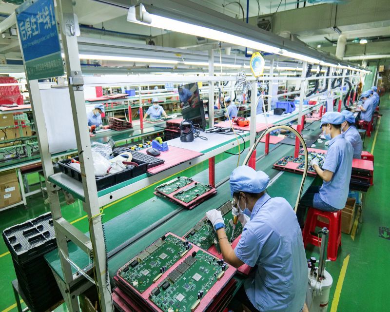
Welcome to Guangzhou Tongsen Electronic Technology Co., LTD. Website!
Why is SMT assembly prevalent?
After completion of the SMT soldering process, it is necessary to remove the residual flux and solder paste as part of the assembly process. This requires the implementation of a printed circuit board cleaning process, which is critical for producing a final product with reliability and purity.
Accelerating Miniaturization Trend
In daily life, we generally don't want items to be "small," but in electronics projects, "small" is a commendable attribute. You'll notice that the electronic products we use daily are trending towards compactness and lightweight design. However, in the old PCB assembly process, we used larger DIP components and employed through-hole mounting methods, which clearly contradicts this trend. To meet the needs of miniaturization and lightweight design, SMT technology was born.
SMT PCBA uses SMD, allowing us to install components using a pick-and-place process. This method enables us to encapsulate components in a smaller space, thus contributing to the creation of lighter, more stylish devices that seamlessly integrate into our projects and daily lives. Through denser component layouts, manufacturers can apply PCBA boards with more functionality across various industries. For example, the Internet of Things (IoT) can achieve cross-departmental and cross-application connectivity of numerous devices through miniaturization.
Improving Electronic Performance
Engineers' efforts are always dedicated to ensuring precise layout accuracy while improving circuit performance. In this context, SMT, through meticulous design, precise component placement, and seamless soldering processes, becomes a key driver of high-performance devices. The connection established between components and the PCB board not only enhances signal quality but also effectively mitigates parasitic factors, thus bestowing the device with commendable performance attributes.

The specific manifestations of SMT's high-performance attributes are found in fields such as automotive, telecommunications, and aerospace. These industries require devices capable of withstanding high operating conditions while maintaining perfect functionality. Through the judicious integration of rigorous testing methods and diligent assembly practices, SMT manufacturing not only meets but exceeds these stringent requirements, significantly expanding the possibilities that can be achieved.
Enhanced Circuit Reliability
This represents an inherent electronic assembly method. The initial phase requires manufacturers to adopt automated SMT pick-and-place machines, thus ensuring process consistency while mitigating the influence of human variables. Subsequently, compared to the through-hole method, this method requires reduced insertion force, thereby reducing circuit board stress and the risk of mechanical damage.
Finally, PCBA facilities employ precision solder connections and stringent quality assurance protocols to maintain the fidelity of the SMT process flow. Undoubtedly, these practices offer significant advantages, particularly in industries such as medical and aerospace, where dependable reliability is paramount.
SMT Assembly Process Flow
Step 1: Stencil Preparation
In the automated SMT PCBA process, one of the key responsibilities of the manufacturer is the fabrication of the PCB stencil, also known as the solder paste stencil or SMT stencil. This stencil takes the form of a stainless steel plate, riddled with apertures, whose positions align with the designated locations of the solder components as specified in the circuit design blueprint. The purpose of this stencil template is to serve as a guide for the precise dispensing of solder paste to the required locations during the assembly process.
Step 2: Solder Paste Printing
The prepared bare PCB is placed within the designated SMT equipment. The corresponding stencil is then strategically positioned atop the component, aligned with the circuit board. Subsequently, solder paste is dispensed onto the apertures of the stencil, using a programmable squeegee for uniform scanning, ensuring that the paste is applied precisely and consistently to the designated solder pads.
Undoubtedly, precision is paramount in the SMT solder paste printing process. The accurate deposition of solder paste is key to ensuring the accuracy of component interconnection and the formation of highly optimized solder joints. The procedural integrity of this phase extends far beyond its scope, as any anomalies (such as misalignment or defects) can trigger complications in subsequent stages of the assembly process.
Step 3: Component Pick and Place
Starting with the IC chip mounting phase, high-speed pick-and-place machines play a central role in orchestrating this meticulous procedure. This phase hinges on the dexterity of robotic arms equipped with sophisticated pick-and-place operations. These arms skillfully retrieve components from feeder tapes and then place them judiciously onto the solder paste-laden PCB pads on the circuit board.
The automated precision exhibited by PCI and advanced pick-and-place machines is a testament to contemporary technological prowess. This technology implements component placement with micron-level accuracy, cleverly ensuring the necessary orientation and alignment. The IC chip mounting process, characterized by its speed and precision, is a cornerstone of modern assembly methods, capable of seamlessly installing thousands of components within an hour.

Step 4: Reflow Soldering
After components are mounted onto the surface of the circuit board, the solder paste, in its molten state, maintains a temporary bond until solidified by a heat source. In SMT board assembly, the transformation of components into integral elements of the circuit board is typically achieved through the reflow soldering process. This method involves controlled heating of the components within a reflow oven, causing the solder paste to liquefy and subsequently form precise solder joints. The key to this process lies in establishing a balance between temperature and duration.
In the reflow soldering process, the molten solder transitions to its solid form upon cooling, achieving both electrical connection and mechanical stability. The orchestration of a carefully controlled heating protocol serves the dual purpose of preventing thermal stress on the components while simultaneously safeguarding their structural integrity.
Step 5: Inspection and Cleaning
Upon completion of the SMT soldering procedure, the removal of residual flux and solder paste is necessary as part of the assembly procedure. This necessitates the implementation of a circuit board cleaning process, which is crucial for producing a final product that boasts reliability and purity. Achieving this perfect outcome hinges on the selection and use of appropriate cleaning agents, including solvents or aqueous solutions. The choice depends on the material composition of the product, ensuring the effective removal of contaminants and residues adhering to the circuit board surface.
Therefore, AOI inspection systems are strategically installed on the production line, responsible for conducting meticulous scans and quality assessments of the PCBAs. This automated inspection, based on advanced optical technologies, detects any anomalies that may require corrective intervention. In such instances, rework becomes necessary, ultimately addressing the identified issues to maintain the stringent standards of the final assembly.
RECOMMENDED NEWS
High-end Custom Services: SMT Chip Processing Meets Diverse Industry Needs


