Welcome to Guangzhou Tongsen Electronic Technology Co., LTD. Website!


How to overcome PCB modeling challenges
As electronic devices become smaller and more prevalent, printed circuit boards (PCBs) and their driving components face increasingly higher power densities and more complex issues. Accurate and detailed analytical methods are necessary to ensure product reliability and performance.
As electronic devices become smaller and more prevalent, printed circuit boards (PCBs) and their driving components face increasingly high power densities and increasingly complex problems. Accurate and detailed analytical methods are necessary to ensure product reliability and performance.
Modeling electronic products is particularly challenging. We usually consider the simulation of large objects to be difficult. However, a simple computer or mobile phone may contain tens of thousands of objects, with a size range of 1000 times (100 micrometers to 100 millimeters), which leads to highly complex models requiring advanced computing power. The PCB itself is a good example.
PCB Modeling Techniques
A PCB has 11 structural layers. Five of these layers are glass fiber reinforced epoxy resin, each with a different glass weave. Six layers consist of thousands of copper traces, pads, and planes, with epoxy resin (also known as dielectric) filling the gaps between the copper features. Both types of layers have thousands of drilled and plated holes, known as through-holes or micro-vias. This complex circuit board geometry results in spatially varying material properties (e.g., elastic modulus, density, thermal conductivity, etc.), which must be accurately specified for any type of simulation.
One step in overcoming these PCB modeling challenges may be to use software specifically designed to capture and process PCB geometry from any electronic computer-aided design (ECAD) file and capable of importing all industry standard output files, including Gerber, ODB++, IPC-2581, and EDB.
Method 1: Lumped or Effective Material Properties
A basic approach to handling the complex geometry of a PCB is to assume "lumped" or "effective" material properties.
The first step in this method involves calculating the orthotropic properties of the glass fiber reinforced laminate layers. When looking at the structural details in Figure 1, you will see various glass weaves in different layers (1078, 2116, etc.). Different glass weaves result in very different material and mechanical behavior, primarily due to different resin content. The elastic modulus (E) and coefficient of thermal expansion (CTE) will vary by more than 40% depending on the laminate structure.
Sherlock can take the material properties of a standard configuration (50% resin/50% glass) listed in the laminate datasheet and calculate the orthotropy of various glass weaves and back out the isotropic properties of the resin.
The next step involves calculating the orthotropy of the copper and resin layers. In this method, the percentage of copper coverage per layer of the board is assumed and the effective orthotropic material properties are calculated.
Method 2: Mapping Material Properties (Trace Mapping)
In this method, a rectangular background mesh is constructed on each layer of the board. Each cell of the background mesh calculates effective orthotropic material properties based on the local concentration of copper and dielectric. This effectively forms a map of material properties for each layer of the PCB.
The calculation of the local properties is similar to Method 1. However, each cell only considers a finite portion of the board, allowing the material map to capture local variations in properties.
The main advantage of trace mapping is the neatness of the mesh and the complete control over mesh density. The mesh can be almost entirely composed of first-order bricks without having to follow the complex geometry of the traces, pads, and planes. For structural mechanics modeling, bricks are preferred over first-order tetrahedral elements because "tets" tend to be overly stiff. The initial element size is between 100 and 500 micrometers, depending on your application (e.g., thermal, mechanical, thermomechanical, etc.). The finer the mesh, the stronger the correlation between trace mapping and the actual geometry.
Trace mapping provides a more accurate representation of the PCB compared to the effective property method detailed in Method 1. It also executes simulations faster and uses fewer resources compared to the method detailed in Method 3 below.
With increasingly complex PCB designs, trace modeling is the method to predict the risk of thermomechanical failure.
Method 3: Detailed Geometry (Trace Modeling)
In stark contrast to the simplicity of Method 1, the analyst can choose to explicitly represent the entire board by extracting the complete 3D geometry of the PCB layout. In this method, fewer assumptions are made about the distribution of materials within the board, as each trace and via is modeled in detail.
With the increasing use of stacked micro-vias and extremely small traces in high-speed circuits, failure to include explicit geometry in more and more applications introduces failure risks during manufacturing, verification testing, and field operation.
However, the challenges of modeling the entire PCB geometry are not insignificant. Not only is the analyst forced to create a large model (potentially exceeding 1M elements per layer), but the complex geometry is either impossible to mesh or filled with undesirable element types and aspect ratios.
To overcome these challenges, Sherlock provides users with a range of options:
Trace modeling (as described above)
Trace modeling regions
Trace modeling enhancements
Trace modeling regions allow users to create solid geometry for each feature within a predefined region. This can reduce the potential size of the model, especially useful where thermomechanical risks exist for specific components, such as ball grid arrays (BGAs) or quad flat no-lead packages (QFNs). This is similar to a local-global modeling approach, but trace modeling regions create a local high-fidelity model within a global low-fidelity model.
Trace modeling enhancement materials are a new feature in Sherlock. Enhancement materials are 2D or 1D elements embedded within 3D structural elements or parent elements. The strain in the enhancement material is calculated based on the displacement field of the embedding element, meaning there is a strong bond between the enhancement material and the surrounding material (mimicking the bond between copper foil and plated copper and epoxy resin).
The advantages of enhancement materials include that the layout geometry does not affect the mesh of the resin or laminate. This provides the analyst with benefits similar to trace mapping, where the mesh is primarily first-order bricks and there is complete control over mesh density.
All these features create exciting opportunities for electrical, thermal, mechanical, and reliability modeling of electronic products for next-generation technologies.
RECOMMENDED NEWS

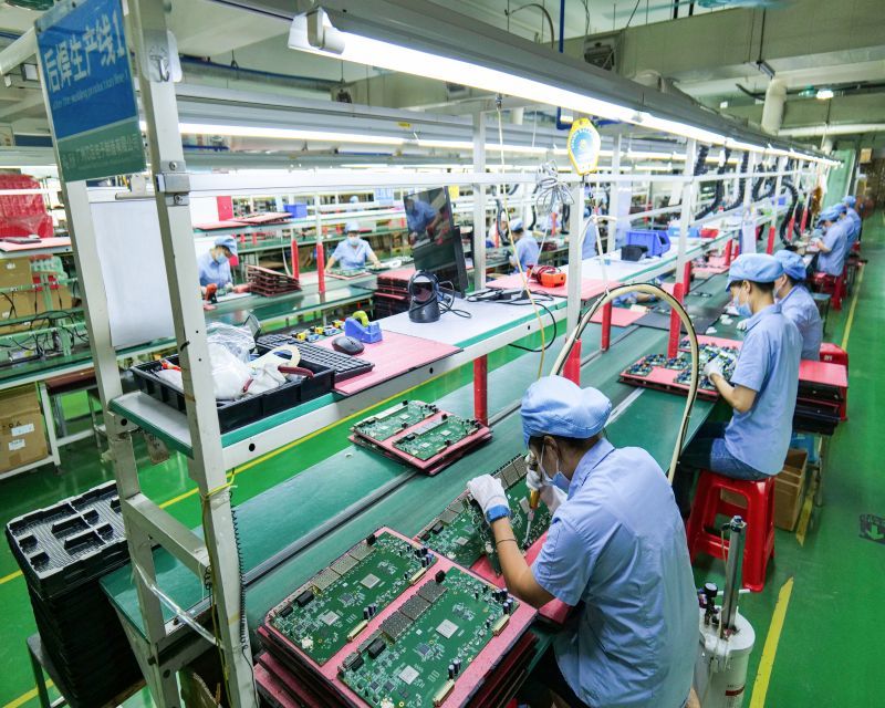
High-end Custom Services: SMT Chip Processing Meets Diverse Industry Needs


(Telephone contact)
Email:
Address: Room 502, Building 1, No. 13, Bohua 4th Road, Huangpu District, Guangzhou City
COPYRIGHT © 2025 Guangzhou Tongsen Electronic Technology Co., Ltd. All rights reserved.