Welcome to Guangzhou Tongsen Electronic Technology Co., LTD. Website!


What is considered a high-speed PCB?
Hardware designers need to know some key techniques. One of them is to reduce the loop area in high-speed PCBs. Due to some issues including EMI and EMC, they must follow basic rules, including reducing loop area, enhancing existing trace return paths, and stitching vias.
What is high-speed PCB design?
The reliability of signals is affected by the physical characteristics of the printed circuit board (PCB). These characteristics include packaging, layout, stacking, and interconnections. High-speed PCB design aims to overcome problems such as radiation, delay, reflection, and crosstalk.
High-speed PCB design is different because it places a strong emphasis on these issues. Most hardware designers are accustomed to designing simple PCBs, focusing all their attention on routing and component placement. However, when using high-speed PCBs, you also need to consider several characteristics.
These are the questions hardware designers need to ask themselves during planning: Where should I place the traces? What is the width? How close are they to the signal? What are the types of components to be connected? These considerations will help you achieve the ideal high-speed PCB design.

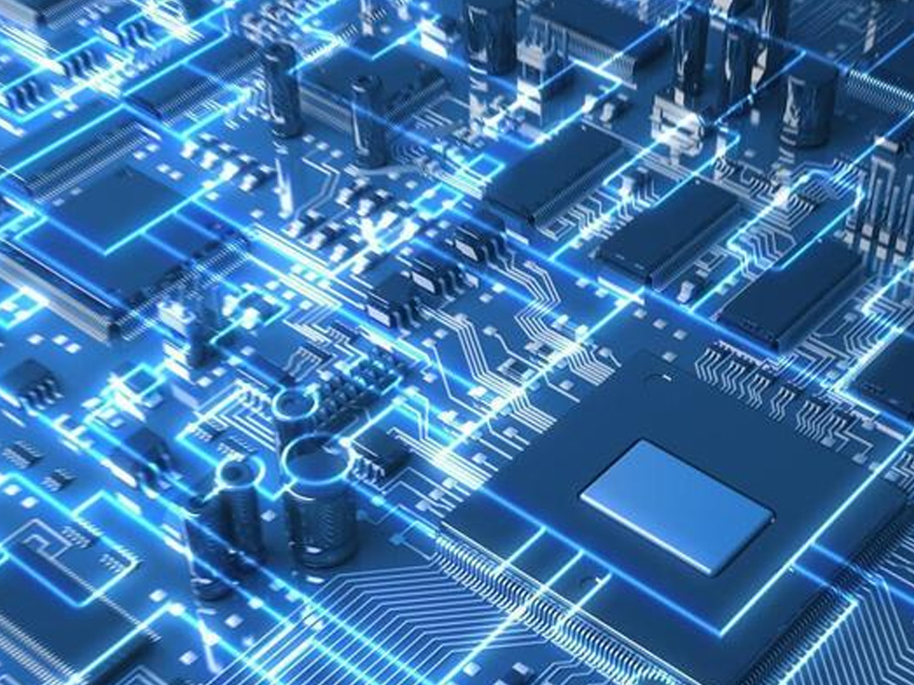
Fundamentals of High-Speed PCB Design
Today, most digital designs use high-speed and low-speed digital protocols. However, high-speed PCBs have RF front ends for wireless connections and interactions. Although most designs start with a schematic, most high-speed
designs focus on interconnect design, routing, and PCB stacking.
How to plan high-speed PCB stacking and impedance?
The process of creating a printed circuit board stack for high-speed boards will define the resistance and wiring. The layers of the PCB stack are dedicated to high-speed signals, ground planes, and power. In addition, various key points need to be considered when allocating layers in the stack.
Board size and new numbers
When performing PCB layout, you should consider the size of the board and the required networks. Large boards will have more area allowing you to access tracks during PCB layout without using multiple signal levels.
Route density
If you are in a situation where there are many networks and the board size is limited to a smaller area, there will not be enough space to route around the surface layer. Therefore, when the routers are pushed closer together, you will need more internal signal layers. If you switch to smaller boards, you can force an increase in routing density.
Interface sum
The perfect strategy is to route a maximum of two interfaces per layer, while considering bus width (series or parallel) and board range. Keeping most of the signals in high-speed digital ports at a uniform level will ensure reliable impedance, and all signals can see the offset.
RF signals and short speeds
Note whether there are any RF signals or low-speed and short-speed digital signals in your design. If so, these signals will occupy more space on the outer layers, which could have been used for high-speed buses or mechanisms, so additional layers may be needed.
Power integrity
The main cornerstone of power reliability is to use excellent power planes and ground planes for each voltage level required for large ICs. These planes should be located on adjacent layers to help ensure excellent plane capacitance, which helps stabilize the power supply using decoupling capacitors.
However, more rules must be considered for all types of high-speed printed circuit boards (PCBs).
The main noise generated by the power distribution network when transmitting power is.
Reduce crosstalk between adjacent traces. When the signal frequency is high, due to the capacitive impedance of the excited existing lines, the feeling of capacitive crosstalk will quickly arise.
Reduce the impact of ground bounce. These effects are closely related to signal integrity issues and can be reduced by properly shaping the PCB stack and separating several parts of the PCB.
Try to get the best possible resistance matching
Provide an appropriate solution for each signal line. This aspect, along with controlling input, load, and transmission impedance, eliminates signal reflections.
Higher degree of radiation and electromagnetic interference (EMI) resistance
What skills are needed for high-speed PCB design?
When hardware designers plan to design high-speed PCBs, they consider some factors and parameters that comply with basic PCB design rules and methods.
Here are some key high-speed PCB design skills:
Having more innovative design software options
Use software that can provide you with some advanced options. Designing high-speed PCBs is not easy. It requires many complex features in CAD software. There may not be many options on various programs. Therefore, you need an in-depth understanding of powerful CAD tools.
High-speed transmission
Excellent designers need to understand basic routing rules. This is one of the basic principles of high-speed routing. It also includes keeping the traces neat and not cutting off the ground plane.
Use impedance power to guide traces
High-speed PCBs require impedance matching to match signals of approximately 40-120 ohms. As for characteristic impedance matching tips, they are transmitters of multiple variance pairs. Hardware designers must know how to measure trace width and layer stack to obtain key impedance values.
Lack of accurate impedance values can have a serious impact on the signal, leading to data being exploited.
Length matching traces
There are a series of lines in interfaces and high-speed memory buses. These lines can operate at fairly high frequencies. Therefore, the signal must move from the sender to the receiver simultaneously. In addition, it also requires a function called length matching. It helps define the tolerance value that needs to be matched in length.
Reduce vulnerabilities
Hardware designers need to understand some key techniques. One of them is to reduce the loop area in high-speed PCBs. Due to some problems including EMI and EMC, they must follow basic rules, including reducing loop area, enhancing existing trace return paths, and stitching vias.
RECOMMENDED NEWS

High-end Custom Services: SMT Chip Processing Meets Diverse Industry Needs


(Telephone contact)
Email:
Address: Room 502, Building 1, No. 13, Bohua 4th Road, Huangpu District, Guangzhou City
COPYRIGHT © 2025 Guangzhou Tongsen Electronic Technology Co., Ltd. All rights reserved.