Welcome to Guangzhou Tongsen Electronic Technology Co., LTD. Website!


Benefits of HDI PCB
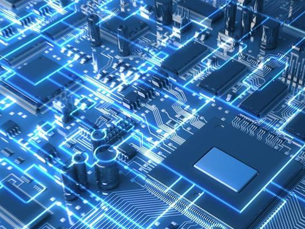
Key Role of Microvia Technology: Microvia technology is the core of HDI PCB design, enabling the creation of complex and dense circuits within a limited space. By utilizing microvias, designers can achieve higher interconnect density while maintaining excellent signal integrity. Understanding and utilizing this technology is crucial to fully realizing the potential of high-density interconnect solutions.
HDI technology has revolutionized the field of PCB design. The steadily increasing demand for high-density interconnect PCBs across various industries has driven the need for a more comprehensive understanding of HDI PCB design. This comprehensive guide aims to provide valuable and in-depth knowledge about the complexities of high-density interconnect PCB design, catering to the growing interest and demand for advanced PCB solutions.
What is an HDI PCB?
Key Features of HDI PCBs
Microvias and Blind Vias: HDI PCBs typically utilize microvias and blind vias, enabling higher interconnect density within the PCB. This capability allows for complex and compact circuit designs, crucial for modern electronic devices.
Enhanced Circuit Density and Signal Integrity: A significant advantage of HDI PCBs is their ability to support higher circuit density while maintaining excellent signal integrity. This capability is essential for meeting the demands of advanced electronic applications where space constraints and performance requirements are paramount.
By integrating microvias and blind vias, high-density interconnect PCBs achieve significant advancements in circuit density and signal integrity, making them an indispensable part of cutting-edge electronic designs.
Understanding HDI Technology
HDI technology plays a crucial role in the evolution of electronic devices, driving significant advancements in PCB design. Understanding the importance of HDI technology is essential for engineers and designers seeking to push the boundaries of compact electronics.
Importance of HDI Technology
Miniaturization of Electronic Devices: HDI technology has facilitated the development of smaller and more efficient electronic devices. By integrating high-density interconnect solutions, manufacturers can significantly reduce the size of electronic products without compromising functionality or performance.
Enhanced Performance of Compact Electronics: The application of HDI technology leads to improved performance and functionality in compact electronic products. This is particularly important in industries such as consumer electronics, wearables, and IoT devices, where space is limited and innovative solutions are needed to maximize performance within confined spaces.
In essence, HDI technology not only enables miniaturization but also enhances the overall performance and functionality of PCBs in compact electronic products. This transformative impact underscores the importance of HDI technology in shaping the future landscape of electronic device design and manufacturing.
HDI High-Density Interconnect PCB Design Principles
HDI PCB Design Considerations
Several key principles and considerations need to be addressed when delving into the realm of high-density interconnect PCB design. These factors are crucial for ensuring optimal performance and functionality of HDI PCBs, especially within the context of modern electronic applications.
Importance of Aspect Ratio: Aspect ratio is a critical factor in HDI PCB design. It refers to the ratio of the depth to the diameter of a via, playing a significant role in determining the reliability and manufacturability of microvias. Engineers must carefully optimize the aspect ratio to ensure robustness while meeting the miniaturization demands of contemporary electronic devices.
Crucial Role of Microvia Technology: Microvia technology is at the heart of HDI PCB design, enabling the creation of complex and dense circuits within a limited space. By leveraging microvias, designers can achieve higher interconnect density while maintaining excellent signal integrity. Understanding and utilizing this technology is crucial for realizing the full potential of high-density interconnect solutions.
In essence, mastering these design considerations is paramount for engineers and designers venturing into HDI PCB design. By carefully studying the complexities of aspect ratio and employing microvia technology, they can pave the way for groundbreaking advancements in the development and manufacturing of compact electronics.

Advantages of HDI PCBs
HDI PCBs offer numerous advantages, making them an integral part of modern electronic design and manufacturing. These advantages include enhanced signal integrity, electrical performance, and the ability to create smaller and lighter electronic devices.
Benefits of Using HDI PCBs
Improved Signal Integrity: High-Density Interconnect (HDI) PCBs are meticulously designed to deliver superior signal integrity, ensuring that electronic signals propagate with minimal loss or distortion. This is particularly crucial in high-frequency applications where signal fidelity is paramount. By minimizing signal attenuation, HDI PCBs contribute to the overall reliability and performance of electronic systems.
Enhanced Electrical Performance: Using HDI PCBs results in improved electrical performance, characterized by reduced impedance and minimized crosstalk between adjacent traces. These attributes are essential for maintaining the integrity of electrical signals, especially in dense circuit layouts where interference can pose significant challenges.
Smaller Form Factor and Lighter Weight: HDI PCBs enable the creation of electronic devices with smaller form factors and lighter weights, addressing the growing demand for compact and lightweight products across various industries. This capability is particularly advantageous in portable electronics, IoT devices, and aerospace applications where space and weight are critical design constraints.
RECOMMENDED NEWS

High-end Custom Services: SMT Chip Processing Meets Diverse Industry Needs


(Telephone contact)
Email:
Address: Room 502, Building 1, No. 13, Bohua 4th Road, Huangpu District, Guangzhou City
COPYRIGHT © 2025 Guangzhou Tongsen Electronic Technology Co., Ltd. All rights reserved.