Welcome to Guangzhou Tongsen Electronic Technology Co., LTD. Website!


What is a PCB and a brief introduction to PCB design
Printed Circuit Board (PCB) design has evolved into a distinct professional field within the electronics industry. PCBs play a vital role as they provide electrical interconnections between electronic components, a rigid support for mounting components, and a compact package that can be integrated into the final product. They are the primary components in electronic devices responsible for form and function, and they allow advanced semiconductors to communicate with each other at high data rates.
Printed Circuit Board (PCB) design has evolved into a distinct professional field within the electronics industry. PCBs play a vital role as they provide electrical interconnections between electronic components, a rigid support for mounting components, and a compact package that can be integrated into the final product. They are the primary components in electronic devices responsible for form and function, and they allow advanced semiconductors to communicate with each other at high data rates.
What is a Printed Circuit Board?
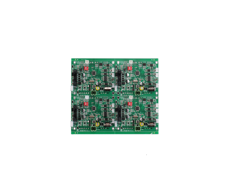
A printed circuit board (PCB) is an electronic component that uses copper conductors to establish electrical connections between components. PCBs also provide mechanical support for electronic components, allowing the device to be mounted in an enclosure.
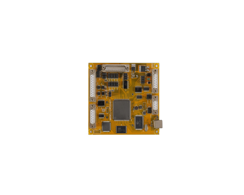
All PCBs are constructed from alternating layers of conductive copper and electrically insulating materials. Conductive features on a printed circuit board include copper traces, pads, and conductive planes. The mechanical structure consists of insulating materials sandwiched between the conductor layers. The overall structure is plated and covered with a non-conductive solder resist layer, which is silkscreened to provide a legend for the electronic components. After these manufacturing steps are complete, the bare board is sent to printed circuit board assembly, where components are soldered to the board and the PCBA can then be tested.
During the manufacturing process, inner copper layers are etched, leaving behind copper traces used to connect components within the board. Multiple etched layers are sequentially laminated until the printed circuit board stackup is complete. This is the overall process used in PCB design manufacturing, where the bare board is formed before going through the printed circuit board assembly process.
Structure and Applications of PCBs
Many important performance characteristics of a PCB are defined in the PCB stackup or layer arrangement. The stackup consists of alternating layers of conductive and insulating materials, as well as alternating core and prepreg layers (two types of dielectric used in the stackup). The dielectric and mechanical properties of the core and prepreg will determine the reliability and signal/power integrity of the design and should be carefully chosen when designing high-reliability applications. For example, military and medical applications require highly reliable designs that may be deployed in harsh environments, while telecommunication systems PCBs may require low-loss PTFE laminates in small form factors.
PCB Design
When starting a new design, a printed circuit board goes through several stages. Production-level boards are designed using ECAD software or CAD applications that include many utilities specifically for board design and layout. ECAD software is designed to help designers through the specific processes of board design, starting from basic electrical schematics to the end of manufacturing file preparation. Board design follows a basic flow:
Front-end engineering - In this stage, the main components are selected and some basic schematics are usually created to design the functionality within the board.
Schematic capture - This is the stage where simple schematics are translated into electronic drawings that define the electrical connections between components using ECAD software. Schematic symbols are used to represent the components in the design.
Material selection and PCB stackup design - In this stage, the laminate material is selected and the stackup is designed to meet the requirements for plane layers, signal layers, dedicated routing channels, and specific material characteristics.
Component placement - After setting the board shape and importing the components into a new PCB layout, the components are arranged in the layout to meet the mechanical requirements of the design.
Routing - Once the component placement is approved, the routing between the components can be done. Routing tools in ECAD software are used to set the routing geometry, and the routing geometry can be determined at this stage to ensure impedance control (for high-speed signals).
Design review and verification - After routing is complete, the design should be checked and evaluated to ensure that there are no errors or unresolved issues. This can be done through manual inspection or by using post-layout simulation tools.
Manufacturing preparation - Once the design is complete, it is time to prepare for production by generating standard manufacturing files. These files are used by automated manufacturing and assembly equipment.
If you want to easily complete all these stages in the PCB electronic board design process, you need to use better design software with an intuitive user interface and complete PCB design capabilities.
Previous :
RECOMMENDED NEWS

High-end Custom Services: SMT Chip Processing Meets Diverse Industry Needs


(Telephone contact)
Email:
Address: Room 502, Building 1, No. 13, Bohua 4th Road, Huangpu District, Guangzhou City
COPYRIGHT © 2025 Guangzhou Tongsen Electronic Technology Co., Ltd. All rights reserved.