Welcome to Guangzhou Tongsen Electronic Technology Co., LTD. Website!


Basic best practices for PCB design
Do not attempt to optimize your design by circumventing the limitations in the decoupling power supply lines and related component datasheets. You can spend as much time installing them as you like, since capacitors are cheap and durable, while following rule 5 and using standard value ranges to keep inventory clean.
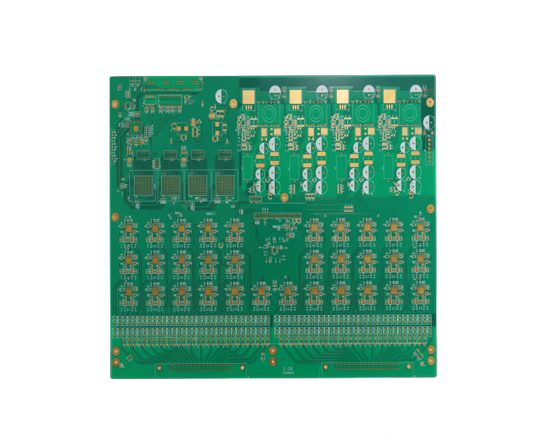
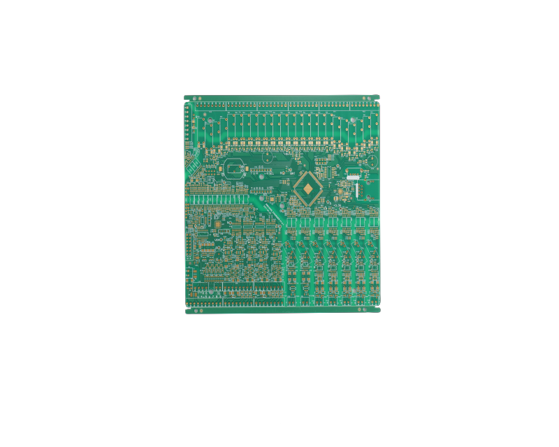
Despite the ever-increasing integration of semiconductors, with readily available system-on-chips and many powerful, ready-to-use PCBs in numerous application fields, customized printed circuit boards are still needed in many applications of personalized electronic products. PCB design is crucial in the development of new projects. PCB design is usually carried out after the circuit board schematic is finalized, combined with project requirements, and can be used to optimize the layout of the target electronic system.
Ten Golden Rules of PCB Design
1: Keep circuit paths short and direct
This sounds simple, but you should always keep this in mind, even if it means altering the PCB design layout to optimize circuit paths. This is especially true for high-speed digital circuits, as its impedance and parasitic effects have a limited impact on system performance.
2: Choose the right grid - pay attention to using a grid spacing that matches reasonably sized components
Since many components have different package sizes, engineers should use components that are more suitable for their design. In addition, polygons are very important for board copper deposition. Polygon fill deviations usually occur on multi-grid PCBs, which are not as standard as single-grid PCBs, but provide board life beyond requirements. While multi-grid seems like a powerful tool, engineers who consider the PCB layout more in the early stages of design can avoid spacing problems and make full use of the circuit board.
3: Place related components and necessary test points together
Place the discrete components required by the project close to the devices, keeping bypass capacitors and resistors in the same location. This helps optimize the line length mentioned in Rule 2 and also makes testing and inspection easier.
4: Use power planes to manage the distribution of power and ground lines
For most PCB design software, a copper-clad power plane is a faster and simpler option. By connecting a large number of conductors together, it ensures efficient current with minimal impedance or voltage drop, while providing sufficient grounding loops. If possible, run multiple power lines in the same area of the board and ensure that the ground plane covers most of the PCB. This facilitates exchange between adjacent layers.
5: Consolidate component values
When sourcing custom PCB components, some discrete components have the same performance characteristics but higher or lower costs. By consolidating a small range of standard values, the bill of materials can be simplified and costs potentially reduced.
6: Design PCB panels
Choosing a laminate size that is more suitable for manufacturer production will help reduce prototyping and production costs. First, arrange the PCB boards on the panel, contact the PCB board manufacturer to understand their dimensions for each panel, then modify your design specifications, and try to repeat your design as much as possible within these panel dimensions.
7. Effectively use silkscreen
Silkscreen is often used by PCB manufacturers to mark some useful information. Not only should functions and test points be clearly marked, but also the orientation of components and connectors should be indicated as much as possible. Making full use of silkscreen technology on the PCB surface can coordinate the entire PCB production process.
8: Perform Design Rule Checks (DRC and DFM) as much as possible
While running the DRC function on PCB software only takes a short time, in more complex design environments, remembering a good habit and performing checks throughout the design process can save a lot of time. Every routing decision is crucial, and performing DRC allows you to understand the most important routing.
9: Decoupling capacitors are needed
Never try to optimize your design by avoiding decoupling power lines and the limitations in the datasheets of related components. You can spend as much time as possible installing them, as capacitors are cheap and durable, while following rule 5 and using a standard value range to keep inventory clean.
10: Generate PCB manufacturing parameters and verify before production
You can export the Gerber files first and then use a free viewer to check if it works as expected to avoid production errors.
As circuit designs are increasingly widely shared and professional teams increasingly rely on advanced designs, the above basic rules will remain indispensable steps in PCB design. We believe this is very important for PCB design. By clarifying these basic rules we have discussed, designers can maximize the value of their products and gain greater benefits from the PCB boards they manufacture.
RECOMMENDED NEWS

High-end Custom Services: SMT Chip Processing Meets Diverse Industry Needs


(Telephone contact)
Email:
Address: Room 502, Building 1, No. 13, Bohua 4th Road, Huangpu District, Guangzhou City
COPYRIGHT © 2025 Guangzhou Tongsen Electronic Technology Co., Ltd. All rights reserved.