Welcome to Guangzhou Tongsen Electronic Technology Co., LTD. Website!


PCB components and types
Printed Circuit Board (PCB) layout is the blueprint guiding the production of circuit boards, which are the backbone of any electronic device. This article explores the core principles of PCB layout, component placement, routing, and signal integrity.
Printed Circuit Board (PCB) layout is the blueprint that guides the production of circuit boards, which are the backbone of any electronic device.
The realm of electronic design is intricately interwoven with the art and science of Printed Circuit Board (PCB) layout. From smartphones to spacecraft, PCBs are the backbone of countless electronic devices, and the way they are designed and manufactured significantly impacts the performance and reliability of these technological marvels. In this comprehensive exploration, we will unravel the multifaceted nature of PCB layout, elucidating the crucial interplay between solder, PCB manufacturing processes, stacking configurations, solder mounting, and board layout, as these elements collectively constitute efficient and reliable electronic systems.
The layout of a PCB resembles a meticulously crafted blueprint, providing a comprehensive map that precisely dictates the placement of fundamental electronic components such as resistors, capacitors, and Integrated Circuits (ICs). It acts as an architectural canvas upon which intricate electrical connections unfold. This complex design blueprint not only dictates where these components must reside but delves into the intricacies of how they harmoniously interact through a complex network of conductive tracks and pads. These conductive pathways are the lifeblood of any electronic system, transmitting signals and power to ensure the seamless operation of the device.
In essence, PCB layout is more than just a design; it's an intricate map that guides the functionality of an electronic device. This process demands a profound understanding of electronic components, circuit theory, and design principles. Therefore, the role of a PCB designer is critical within the electronics industry. They must possess a solid electronics foundation, proficiency in PCB design software, and a keen eye for detail to ensure that the layout is not only accurate but also efficiently serves its intended purpose.
Fundamentals of PCB Design
PCB design is a complex process involving multiple stages, from conceptualization to final production. It begins with the creation of a schematic, which is a symbolic representation of the circuit. This diagram includes all the components that will be part of the circuit and their interconnections. The schematic serves as a guide for the PCB layout, which is the physical representation of the circuit.
The role of a PCB designer is multifaceted. They are responsible for translating the schematic into a functional PCB layout. This involves determining the placement of components, routing interconnections, and ensuring that the design adheres to industry standards and guidelines. Designers must also consider factors such as the electrical requirements of the circuit, the physical constraints of the PCB, and the manufacturing process.
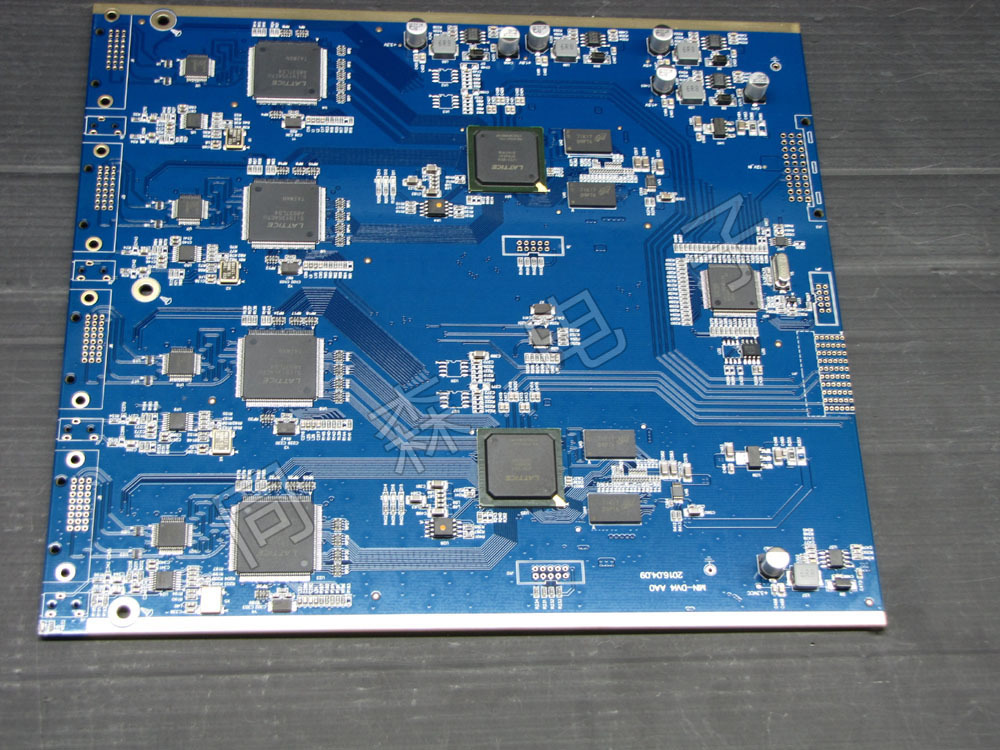
Components of a PCB
A PCB is composed of multiple components, each serving a specific function. The primary component is the board itself, typically made of a non-conductive material such as fiberglass or plastic. This board serves as the foundation for mounting other components.
Resistors are common components on a PCB. They regulate the flow of current in a circuit by offering resistance. The resistance value of a resistor (measured in ohms) determines the extent to which it resists the current.
Capacitors are another type of component. They store and release electrical energy, acting somewhat like a battery. Capacitors are crucial for filtering power noise, blocking direct current (DC) while allowing alternating current (AC) to pass, and many other functions.
Integrated Circuits (ICs) are essentially miniature circuits that perform specific functions. These circuits range from simple logic gates to complex microprocessors. ICs are typically the complex components on a PCB, often dictating the overall functionality of the device. Conductive tracks and pads connect all these components. These tracks, usually made of copper, are etched onto the board during the design process. They provide pathways for current to flow between components. Pads are small exposed portions of metal to which components are soldered onto the board. Each component plays a vital role in the overall functionality of the PCB. The layout and interconnection of these components determine the performance of the circuit and how the electronic device operates.
Types of PCBs
There are various types of PCBs, each suited for different applications based on their physical and electrical characteristics.
Single-sided PCBs are the simplest type. They have components on one side of the board and conductive copper tracks on the other. They are typically used in simple electronic devices where space and complexity are not major concerns, such as power supplies and radios.
Double-sided PCBs have conductive copper tracks on both sides of the board. This allows for higher component density and interconnections, making them suitable for more complex devices. The two sides are connected using through-hole technology, where holes are drilled in the board and filled with conductive material to establish electrical connections.
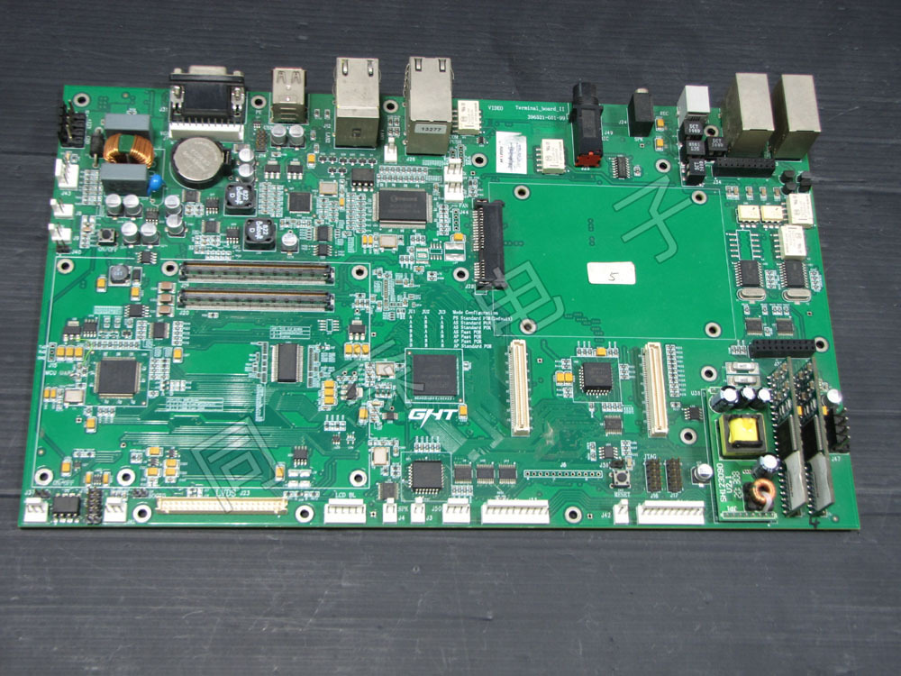
Multilayer PCBs further develop this concept by separating multiple layers of conductive tracks with insulating layers. Multilayer PCBs range from 4 to 12 layers, or even more in high-density designs. These layers are connected using through-hole connections, similar to double-sided PCBs. Multilayer PCBs are used in highly complex devices such as computers and medical equipment where space is at a premium and high levels of electrical performance are required.
Rigid PCBs are made from sturdy substrate materials such as fiberglass, which allows them to maintain their shape. They are strong and durable, capable of supporting heavy components, but they cannot be bent or flexed. They are commonly used in desktop computers and other stationary electronic devices.
In contrast, flexible PCBs are made from flexible plastic or materials such as Kapton. They can be bent and stretched without damaging the circuitry. This makes them ideal for devices such as cameras and mobile phones where the PCB needs to fit into compact, irregularly shaped enclosures.
Each type of PCB presents unique advantages and challenges in terms of design, manufacturing, and application. The choice of PCB type depends on the specific requirements of the electronic device being designed, including its complexity, physical constraints, and performance requirements.
Previous
Previous :
Next :
RECOMMENDED NEWS

High-end Custom Services: SMT Chip Processing Meets Diverse Industry Needs


(Telephone contact)
Email:
Address: Room 502, Building 1, No. 13, Bohua 4th Road, Huangpu District, Guangzhou City
COPYRIGHT © 2025 Guangzhou Tongsen Electronic Technology Co., Ltd. All rights reserved.