Welcome to Guangzhou Tongsen Electronic Technology Co., LTD. Website!


What is the PCB manufacturing process?
To fully leverage DFM to prevent unnecessary time delays and added manufacturing costs, you need to employ a thorough and robust PCB design analysis. With software packages such as documentation automation tools, you can create multiple detailed views to aid your CM during PCB manufacturing.
What is the PCB manufacturing process?
Jumping straight into manufacturing without understanding the relationship and steps between the schematic or idea in your mind and the realization of that idea won't be helpful. Before defining PCB manufacturing, it may be helpful to define a few other terms and their interrelationships.
PCB Development: PCB development can be defined as the process of moving a circuit board design from the design phase to the production phase. This typically involves three phases: design, manufacturing, and testing. Except for simpler designs, this process is iterative, aiming to achieve the highest quality design within the stipulated development time.
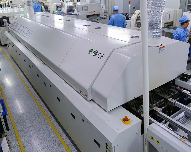
PCB Manufacturing: PCB manufacturing is the construction of the circuit board design. This is a two-step process, beginning with circuit board fabrication and ending with printed circuit board assembly (PCBA).
PCB Testing: PCB testing, sometimes called bring-up, is the third phase of PCB development; it takes place after manufacturing. Testing during the development process aims to assess the board's ability to perform its intended operational functions. Any errors or areas where the design needs modification to improve performance will be identified at this stage, initiating another cycle to incorporate design changes.
PCB Assembly: PCB assembly, or PCBA, is the second step or phase of PCB manufacturing where board components are mounted onto the bare board via a soldering process.
With that in mind, what is the PCB manufacturing process?
PCB Manufacturing Process
PCB manufacturing is the process or procedure of converting a circuit board design into a physical structure according to the specifications provided in the design package. This physical manifestation is achieved through the following operations or techniques:
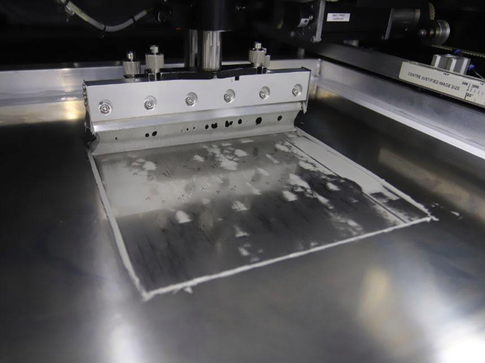
Imaging the required layout on the copper clad laminate board;
Etching or removing excess copper from the inner layers to expose the traces and pads;
Creating the PCB layer stack-up by laminating (heating and pressing) the board materials at high temperature;
Drilling holes for mounting holes, through-hole pins, and vias;
Etching or removing excess copper from the surface layer to expose the traces and pads;
Plating the vias and through-holes;
Adding a protective coating or solder mask to the surface;
Screen printing reference and polarity indicators, markings, or other labels on the surface;
Optionally, adding a finish to the copper areas on the surface;
Now, let's see what this information means for PCB development.
Is understanding the PCB manufacturing process important?
One could, and probably should, ask the question: “Is understanding the PCB manufacturing process important?” After all, PCB manufacturing isn’t a design activity, but an outsourced activity performed by a contract manufacturer (CM). While manufacturing is indeed not a design task, it strictly adheres to the specifications you provide to the CM.
In most cases, your CM doesn’t understand your design intent or performance goals. Therefore, they won’t know if you’ve made the right choices in terms of materials, layout, via locations and types, trace parameters, or other board factors that are set during manufacturing and can affect your PCB’s manufacturability, production yield, or post-deployment performance, as follows:
Manufacturability: The manufacturability of your board depends on several design choices. These include ensuring sufficient clearance between surface mount components and the board edges, and that the coefficient of thermal expansion (CTE) of the chosen materials is high enough to withstand PCBA, especially lead-free soldering. Both situations could result in your board being unmanufacturable without redesign. Furthermore, if you decide to panel your design, this also requires careful consideration.
Yield: Your board may be manufacturable, but there are issues during the manufacturing process. For example, specifying parameters outside the capabilities of the CM’s equipment could result in an unacceptable number of unusable boards.
Reliability: Depending on the intended use of your board, it is classified according to IPC-6011. For rigid PCBs, there are three classification levels that set specific parameters the board construction must meet to achieve the specified level of performance reliability. If your board is classified below your application requirements, it could lead to inconsistent operation or premature board failure.
Therefore, the answer is yes! Understanding the PCB manufacturing process is very important because the design choices you make at this stage will have implications throughout the PCB development, production, and even operation. The best way to avoid problems resulting from not incorporating knowledge of the PCB manufacturing process into your design decisions is to utilize manufacturing-focused design (DFM) rules and guidelines based on CM capabilities.
To fully leverage DFM to prevent unnecessary time delays and added manufacturing costs, you need to employ comprehensive and robust PCB design analysis. With software packages such as documentation automation tools, you can create multiple detailed views to aid your CM during the PCB manufacturing process.
Previous
RECOMMENDED NEWS

High-end Custom Services: SMT Chip Processing Meets Diverse Industry Needs


(Telephone contact)
Email:
Address: Room 502, Building 1, No. 13, Bohua 4th Road, Huangpu District, Guangzhou City
COPYRIGHT © 2025 Guangzhou Tongsen Electronic Technology Co., Ltd. All rights reserved.