Welcome to Guangzhou Tongsen Electronic Technology Co., LTD. Website!


The most basic steps in PCB copy board production
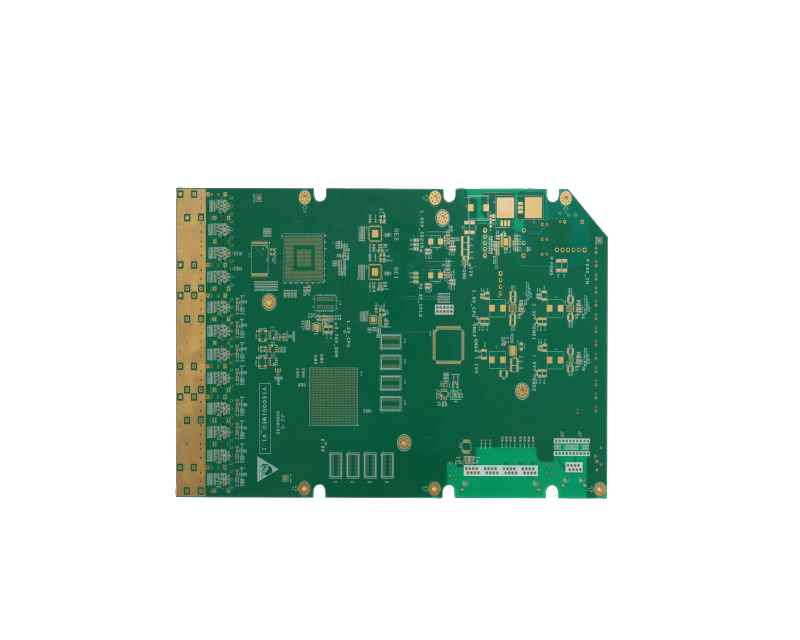
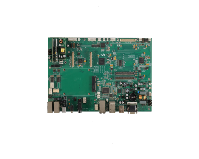
The manufacturing process of PCB copying has developed rapidly. Different types and requirements of PCBs use different processes, but the basic process flow is the same. It generally involves processes such as film making, pattern transfer, chemical etching, via and copper foil processing, welding, and solder resist processing.
The manufacturing process of PCB copying has developed rapidly. Different types and requirements of PCBs use different processes, but the basic process flow is the same. It generally involves processes such as film making, pattern transfer, chemical etching, via and copper foil processing, soldering, and solder resist processing.
The PCB copying production process can be roughly divided into the following four steps:
Preliminary PCB Copying Production
1. Draw the base map
Most base maps are drawn by designers. To ensure the quality of printed circuit board processing, PCB manufacturers must check and modify these base maps. If they do not meet the requirements, they need to be redrawn.
2. Phototypesetting
Use the drawn circuit board base map to make a photoplate, with the layout size consistent with the PCB size.
The PCB phototypesetting process is roughly the same as ordinary photography and can be divided into: film cutting-exposure-development-fixing-washing-drying-retouching. Before taking photos, check the correctness of the base map, especially the base map that has been placed for a long time.
Before exposure, the focal length should be adjusted, and the focal lengths of the two plates should be kept consistent; after the photographic film is dried, it also needs to be corrected.
PCB Production Graphic Transfer Two Steps
Transferring the PCB printed circuit pattern on the photoplate to the copper-clad board is called PCB pattern transfer. There are many methods for PCB pattern transfer, and the commonly used ones are screen printing and photochemical methods.
1. Screen Leakage
Screen printing is similar to offset printing. A layer of paint or glue is attached to the screen, and then the printed circuit diagram is made into a hollow pattern according to technical requirements. Screen printing is an ancient printing technology, simple to operate, and low in cost; manual, semi-automatic, or fully automatic screen printing machines can be used to achieve this. The manual screen printing steps are as follows:
1) Position the copper-clad board on the base plate, and place the printed material in the frame of the fixed screen.
2) Use a rubber plate to scrape off the embossed material, so that the screen is in direct contact with the copper-clad board, and a composite pattern is formed on the copper-clad board.
3) Then dry and modify.
PCB Production Third Optical Method
(1) Direct photosensitive method
The process is: surface treatment of the copper-clad board → photosensitive resin coating → exposure → development → film formation → plate repair. Plate repair is a necessary step before etching. Burrs, broken lines, and pinholes can all be repaired.
(2) Photosensitive dry film method
Its process is the same as the direct photosensitive method, but it does not use photosensitive resin, but uses a thin film as the photosensitive material. This thin film is composed of three layers of materials: polyester film, photosensitive film, and polyethylene film. The photosensitive film is sandwiched in the middle. When used, the outer protective film is peeled off, and the photosensitive film is attached to the copper-clad board using a laminating machine.
(3) Chemical etching
It uses chemical methods to remove unnecessary copper foil on the circuit board, leaving the pads, printed lines, and symbols that make up the pattern. Commonly used etchants include acidic copper chloride, alkaline copper chloride, and ferric chloride.
PCB Production Fourth Step, Via and Copper Foil Processing
1. Metallized holes
Hole metallization is the deposition of copper on the hole walls that penetrate the conductors or pads on both sides, making the originally non-metallized hole walls metallized, also called copper plating. In double-sided and multilayer PCBs, this is an indispensable process.
In actual production, a series of processes such as drilling, degreasing, roughening, immersion cleaning solution, hole wall activation, chemical copper plating, electroplating, and thickening are required.
The quality of metallized holes is very important for double-sided PCBs, so it must be inspected. The metal layer is required to be uniform and complete, and the connection with the copper foil is reliable. In surface mount high-density boards, this metallized hole uses a blind hole method (copper filling the entire hole) to reduce the area occupied by the vias and improve the density.
2. Metal coating
In order to improve the conductivity, solderability, wear resistance, decorativeness, and service life of the PCB, and improve the electrical reliability of the PCB printed circuit, metal plating is often performed on the copper foil of the PCB. Commonly used plating materials include gold, silver, and lead-tin alloys.
PCB Production Fifth Step Soldering and Solder Resist Processing
After the PCB copying is coated with metal, a soldering agent or solder resist can be applied according to different needs. Applying a soldering agent can improve solderability; while on high-density lead-tin alloy boards, in order to protect the board surface and ensure the accuracy of soldering, a solder resist can be added to the board surface, so that the exposed pads and other parts are under the solder resist. The solder resist coating has two types: thermosetting and photocuring, and the color is dark green or light green.
RECOMMENDED NEWS

High-end Custom Services: SMT Chip Processing Meets Diverse Industry Needs


(Telephone contact)
Email:
Address: Room 502, Building 1, No. 13, Bohua 4th Road, Huangpu District, Guangzhou City
COPYRIGHT © 2025 Guangzhou Tongsen Electronic Technology Co., Ltd. All rights reserved.