Welcome to Guangzhou Tongsen Electronic Technology Co., LTD. Website!


Trends and Challenges in PCB Manufacturing
To improve signal integrity, clear isolation between analog and digital circuits in the PCB layout is essential. Implementing a thermal management scheme avoids hot spots and improves heat dissipation. Since wireless connectivity is common in IoT circuits, PCB design must meet RF requirements and radiation certifications.
New technological innovations such as 5G connectivity, IoT sensors, and artificial intelligence have helped the printed circuit board (PCB) manufacturing industry to develop significantly, but there are still some challenges to overcome.
In the past, manufacturing circuit boards involved either additive manufacturing methods or subtractive manufacturing methods. However, product designers and contract manufacturers quickly realized the benefits of using both methods in a hybrid process. The rapid turnaround of additive manufacturing methods, along with the robust subtractive manufacturing processes, allows for the creation of reliable and repeatable electronics. Manufacturing steps have steadily advanced, and today, complex PCBs can be produced.
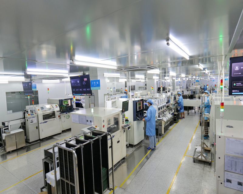
Printed Circuit Board_PCB Manufacturing
Multilayer PCBs with high-density interconnect (HDI), flexible printed circuits, miniature components, high-frequency PCBs, and green PCBs are some of the current trends impacting the PCB market. One widely observed trend is the miniaturization of electronics. PCB manufacturers are constrained to assemble small, powerful components such as miniature BGAs and nano ICs on compact boards. Conversely, the growing demand for high-power circuits in alternative energy solutions such as electric vehicles and solar panels is driving larger PCB designs. Here, the priority is not the board size but its stable performance in harsh operating environments.
In this article, we will discuss some PCB manufacturing trends and their challenges.
HDI PCB
HDI PCBs are widely used in aerospace, automotive, and miniaturized application devices. They are extensively used in medical devices (such as miniature implants) and diagnostic tools (such as CT scanners).
HDI PCBs have a higher wiring density per unit area, significantly reducing product size and weight. Blind and buried via integration greatly reduces stray capacitance and inductance, is compatible with small-pitch IC packaging, has high reliability, and supports high-speed signal transmission.
However, there are still some challenges in manufacturing and assembling HDI PCBs. For tiny pad sizes, component placement requires extra precision. Due to the higher trace density in the circuit, crosstalk or noise issues may arise. In HDI PCBs, selecting the appropriate prepreg material is crucial for achieving accurate laser drilling. Otherwise, the holes may be improperly shaped and of poor quality.
High-Power PCB
The rapid depletion of non-renewable energy sources and their environmental impact highlight the importance of clean energy. Applications such as solar inverters and electric vehicles use high-power PCBs. Typical voltage requirements for solar panels are around 24 V or 48 V, and for motors, they are around 280 V or 360 V. They are also used in heavy machinery, transformers, and other power circuits.
Some of the considerations when designing high-power PCBs are excessive heat dissipation, user safety, and product durability. These PCBs are thicker and include thick copper traces to support high-voltage designs. Power requirements must be estimated and appropriate airflow designed to avoid overheating. It is advisable to add fail-safe circuits. To ensure quality performance, follow industry standards for high-power designs.
IoT in PCBs
Today, the Internet of Things (IoT) is one of the rapidly growing trends in the electronics market. Its design includes three main components: sensors, power circuits, and wireless connectivity. PCB designs supporting IoT functionality must consider some key characteristics. Analog signals captured from IoT sensors should not be coupled with power signals or any other wireless interface signals. Flexible PCBs using HDI technology are a good choice for supporting smaller modern sensors.
To improve signal integrity, clear isolation of analog and digital circuits in the PCB layout is essential. Implementing a thermal management scheme avoids hotspots and improves heat dissipation. Since wireless connectivity is common in IoT circuits, the PCB design must obtain RF requirements and radiation certifications.
IoT devices rely on battery power; therefore, power circuit design is critical for this PCB. The power consumption of each module should be estimated and maintained to extend battery life. In addition, the network connectivity of IoT devices may expose them to the risk of data theft, so it is crucial to implement encryption algorithms and add security features at the PCB level.

Recyclable PCBs
With the global push for green manufacturing, sustainable PCB designs have gained attention. Traditional PCBs contain metals and chemicals that are harmful to the environment. Recycling technologies are inefficient and the process is cumbersome. Researchers are exploring new composite materials that are easy to recycle. Biodegradable polymers are used as binders in PCB manufacturing. This can replace the currently used toxic thermosetting resins in PCB manufacturing. However, biodegradable substrates cannot withstand subtractive processes such as etching and chemical cleaning.
Conversely, additive manufacturing methods are more promising for recyclable PCBs. 3D printed electronics using inkjet and laser printing can reduce manufacturing steps compared to subtractive manufacturing methods. Additive manufacturing processes can easily print complex designs on thin substrates.
Flexible PCBs
With the rise of miniature electronics using unconventional packaging, flexible printed circuit boards have captured a significant market share in the PCB industry. They can be bent and are suitable for various shapes and sizes. Flexible PCBs can operate stably under high-temperature environments. The reliability and light weight of this board make it ideal for aerospace, medical, automotive, and commercial electronics.
Flexible PCBs are driving thinner and lighter structures, suitable for printing technologies using additive processes. Significant advances have been made in the materials and technologies used in flexible PCB manufacturing, but increased material costs and complex assembly procedures are major challenges. They require appropriate storage facilities, otherwise they are easily damaged. Repairing flexible PCBs is both difficult and expensive.
Conclusion
It is necessary to understand the current trends and challenges in the PCB manufacturing industry to improve output and generate revenue. PCB designers and manufacturers must leverage their domain knowledge and train their employees. Assessing consumer needs based on trending technologies can strengthen your product strategy and roadmap. Furthermore, by understanding potential problems, you can prepare for contingencies and reduce the cost and time of product launches.
Previous
RECOMMENDED NEWS

High-end Custom Services: SMT Chip Processing Meets Diverse Industry Needs


(Telephone contact)
Email:
Address: Room 502, Building 1, No. 13, Bohua 4th Road, Huangpu District, Guangzhou City
COPYRIGHT © 2025 Guangzhou Tongsen Electronic Technology Co., Ltd. All rights reserved.