Welcome to Guangzhou Tongsen Electronic Technology Co., LTD. Website!


A Guide to Understanding PCBA Electronics Manufacturing Processes
If required by the client, the next step in the process is to test your printed circuit board to ensure it functions correctly. This includes testing the quality of the PCB connections and testing it using a test fixture. Its functionality under normal operating conditions will be checked. If necessary, the PCB must pass the testing phase before it can be considered complete and sent to you for use in the final product.
The world of electronics and electronics manufacturing is constantly changing. It's a fast-growing industry with no signs of slowing down, and the Printed Circuit Board Assembly (PCBA) process is one of the standards in this rapid development.
Project managers need a reliable Electronics Contract Manufacturer, or ECM, for a stable and proven PCBA process that can handle the advancements in electronics and the components that control electronics PCBs. Before finding an ECM partner to handle your project, you should truly understand how your printed circuit boards are made from quote to prototype to finished product. Here is a guide to understanding the PCBA process.
Quotation Phase
Believe it or not, the quotation phase can be a significant factor in the success of your PCBA project. The quote you receive from the ECM details the time requirements, costs, and specifics of the finished product. Your ECM will check your PCB design for inaccuracies and outdated components. Based on your design, assembly requirements, bill of materials, and other basic project information you provide, your ECM will provide you with a Design for Manufacturing (DFM) analysis. The DFM analysis from the ECM can help with redesign and/or design that saves time and money, reducing the manufacturing cost of the PCB. The goal here is to address potential problems, and the design phase is where it's inexpensive to address them.
Prototype Phase
The project manager takes over in the prototype phase. This is a crucial phase in project development. It ensures your design works perfectly before the printed circuit board goes into full production. The prototype allows the ECM to ensure all parts are in-house before production begins and allows you to test the functionality of the PCB. Prototyping can also help save money by eliminating failures early on. It avoids the cost of faulty boards throughout the entire production run by detecting defects in the production process. Once you are satisfied with the prototype, your project is almost ready for full production.
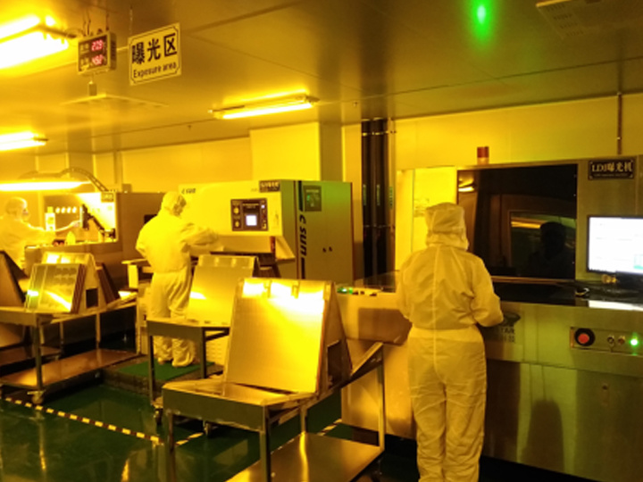
Soldering Phase
The soldering phase of PCB assembly uses two types of assembly: Pick and Place Surface Mount Technology (SMT) and Through-Hole Technology (THT).
Pick and Place
Surface Mount Technology (SMT) is a newer method of producing electronic circuits where components are directly mounted or placed on the surface of a printed circuit board (PCB). A robotic device called a pick-and-place machine places the surface mount components or devices (SMDs) onto the prepared PCB. The SMDs are then soldered to the surface of the board. Most non-connector components on modern PCBs are SMDs.
Through-Hole Technology
Through-hole technology refers to a method of mounting electronic components that involves using leads on the components, which are inserted into holes drilled in the printed circuit board and soldered to pads on the other side. This can be done by hand assembly or using a wave soldering machine. Every component on a board was a through-hole component from the 1950s until the mid-1980s when SMT became popular.
Both technologies can be used on the same board. Through-hole technology will be used for components that are not suitable for surface mounting, such as large transformers and heat-sinked power semiconductors.

Inspection
Once the components are soldered in place, your PCB goes into the inspection phase. Checking for errors and misalignments ensures that errors are found and fixed as quickly as possible. This helps manufacturers and designers save time, labor, and materials. A comprehensive inspection method for modern boards may be Automated Optical Inspection (AOI). The smaller and more complex circuits manufactured today are nearly impossible to detect internal defects through manual inspection. AOI machines use a series of high-powered, automated cameras to scan devices to look for missing components or quality issues and check the quality of the solder joints. AOI performs this at a very high speed, enabling it to process a large number of PCBs in a relatively short time.
Testing
The next step in the process, if required by the customer, is to test your printed circuit board to ensure it works correctly. This includes testing the quality of the PCB connections and testing it using a test fixture. It will check its functionality under normal operating conditions. If required, the PCB must pass the testing phase to be considered complete and sent to you for use in the final product.
RECOMMENDED NEWS

High-end Custom Services: SMT Chip Processing Meets Diverse Industry Needs


(Telephone contact)
Email:
Address: Room 502, Building 1, No. 13, Bohua 4th Road, Huangpu District, Guangzhou City
COPYRIGHT © 2025 Guangzhou Tongsen Electronic Technology Co., Ltd. All rights reserved.