Welcome to Guangzhou Tongsen Electronic Technology Co., LTD. Website!


Multilayer PCB Design: Unveiling HDI Stacking
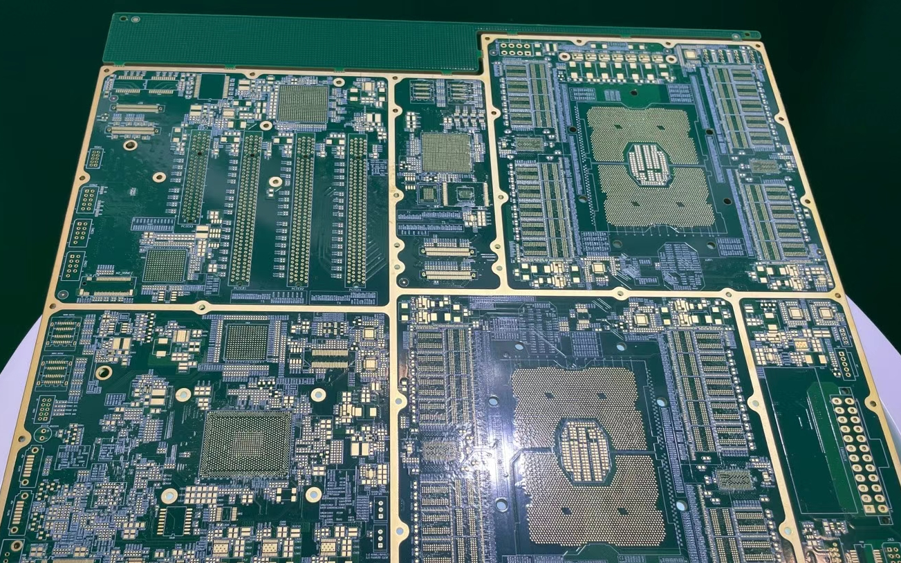
The design of multilayer HDI PCB stacks considers the specific application. They are designed to support the application needs of different electronic systems. They can be used for a variety of purposes, from high-frequency RF circuits to low-voltage power supplies.
When designing a PCB, multilayer PCB stacking is one of the important decisions. It ultimately determines the path of electrical signals through the PCB and the speed at which these signals are transmitted. Many key considerations when choosing a stack include the complexity of the termination scheme required. Each choice has trade-offs. After this discussion, you should have a basic understanding of the stacks used in HDI PCB design.
HDI PCB Stacking
HDI PCB stacking is a method of stacking HDI boards on top of each other from top to bottom and securing them together using prepreg. This is typically done using glass fiber or carbon fiber reinforced plastic (GRP).
Holes are drilled in the top and bottom layers according to a predetermined pattern and spacing. The holes are then enlarged to a diameter larger than the fastener (typically 3/16 inch or 1/4 inch) so that they can be tapped into place using an anti-seize compound. The fasteners will then hold all the layers together during curing.
This stacking method allows for the construction of more complex shapes than manual lamination. However, it requires additional equipment such as a drill press (or at least a drill bit), reamer, tap, and a jig for screwing the fasteners into place.
Multilayer HDI PCB Stacking
There are many types of HDI PCB stacking. Some are more common than others, but each has its uses in the design process.
A common type of HDI PCB stacking is called multilayer stacking. This means that there will be multiple layers of copper within the board. They can be stacked vertically or horizontally, depending on the specific requirements of the design. A common configuration is that the bottom layer contains the ground plane and other components that need to be connected for power distribution. The next layer is the power plane, on top of which are the signal traces. These three layers are then connected using vias (holes drilled through the board), so you can connect different layers without using jumpers or other methods that can cause signal integrity issues.
Multilayer HDI PCB stacking can be done using through-hole technology or surface mount technology (SMT). The choice between these two methods depends on how much space is available on the board and what components need to be mounted. Through-hole mounting requires more space than SMT mounting, so if you are using larger components or want to mount many devices on the board, then SMT may be better suited to your needs.
The main structures of HDI PCB stacking include:
Conductive metal layers (aluminum or copper alloy) are used as ground planes.
Signal layers (copper foil) are used for signal transmission.
Dielectric layers (prepreg) separate the above two layers to prevent them from contacting each other.
Ground layer (screen printing layer) ensures that parts of the board are electrically connected to the ground plane via conductive metal.
Insulating layer (glass fiber cloth) acts as interlayer insulation.
Solder mask layer (satin solder mask) protects components from corrosion during soldering.
Uses of Multilayer HDI PCB Stacking
Multilayer HDI PCB stacking is designed with specific uses in mind. They are designed to support the application needs of different electronic systems. They can be used for a variety of purposes, from high-frequency RF circuits to low-voltage power supplies. Here are some examples:
Large Ground Planes
Large ground planes are an important feature of any high-performance circuit board. It allows for better heat dissipation and provides a larger surface area for signal transmission. However, as you add more and more layers to your ground plane, it becomes increasingly difficult to drill holes in it. With multilayer HDI stacking, you can have large ground planes without worrying about drilling holes in them.
High-Frequency Circuits
High-frequency circuits require shorter trace lengths between components to minimize signal attenuation caused by capacitance. Multilayer HDI stacking allows for very tight routing without increasing parasitic inductance or capacitance. This helps improve the performance of the board at high frequencies.
High-Density Interconnects
High-density interconnects provide more routing options while eliminating vias (used when multiple components need to be connected on a single layer of copper foil). This eliminates fragile connections on the board itself and places them inside the connector so they don't fail, reducing costs and improving reliability.

Important Considerations for Multilayer HDI PCB Stacking
Multilayer HDI PCB stacking is very complex and requires a lot of preparation. Designers must consider different factors when designing, such as:
Number of Layers
The number of layers in an HDI board depends on the application, but is typically between 2 and 6 layers.
The number of layers in an HDI board depends on its size and complexity; therefore, it is recommended to start with small designs before moving on to larger ones.
Layer Organization
Layer organization on an HDI board is critical to its performance, as you must consider all possible failure scenarios during production or operation.
For example, if you have three layers, two cores, and one ground plane, and there are no vertical interconnects between them, then if one layer fails, all other layers will also be affected by this failure because they are not vertically connected via vias (no current flow).
Layer Thickness
The thickness of each layer may vary depending on the application. For example, if you need to have a thicker ground layer on your board, you can add more copper than usual (typically 0.6 mm). If you want finer traces, use less copper (0.2 mm).
Final Thoughts
If you are designing complex HDI PCBs, we hope this guide has been helpful. Multilayer factors can make or break the final product, and understanding the impact of each layer beforehand is a simple way to keep the design simple.
RECOMMENDED NEWS

High-end Custom Services: SMT Chip Processing Meets Diverse Industry Needs


(Telephone contact)
Email:
Address: Room 502, Building 1, No. 13, Bohua 4th Road, Huangpu District, Guangzhou City
COPYRIGHT © 2025 Guangzhou Tongsen Electronic Technology Co., Ltd. All rights reserved.