Welcome to Guangzhou Tongsen Electronic Technology Co., LTD. Website!


What is PCB assembly using SMT technology?
A printed circuit board assembly (PCBA) refers to a finished circuit board with all components soldered and mounted onto a printed circuit board (PCB). The PCB is formed by conductive pathways etched onto a copper-clad laminate for use within a non-conductive substrate. Connecting electronic components to the PCB is the final step in creating a fully functional electronic device.
A printed circuit board assembly (PCBA) is a finished circuit board with all components soldered and mounted onto a printed circuit board (PCB). The PCB features conductive pathways etched onto a copper-clad laminate for forming components within a non-conductive substrate. Connecting electronic components to the PCB is the final step in creating a fully functional electronic device.
What does a printed circuit board assembler do?
A circuit board assembler prepares circuit boards by soldering electronic components onto a printed circuit board (PCB). Reading wiring diagrams, following templates, selecting electronic components, and using hand tools to complete the board are all part of this job.

PCB Assembly Techniques
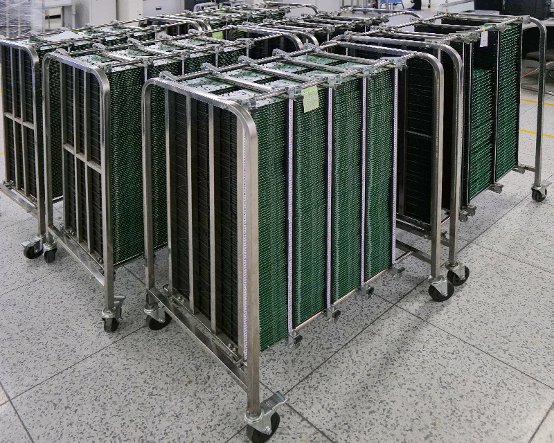
Assembling printed circuit boards requires not only the raw components and a carefully designed board, but also the right techniques. In this case, there are several options to choose from, each with different effects. For example, there is surface mount technology (SMT), as well as manual soldering and the use of pick-and-place machines.
While some PCB assembly processes only require one technique, others require a combination of two or more. For example, many boards require a combination of through-hole technology (THT) and surface mount technology. Understanding when, where, and how to integrate these techniques is a key consideration when choosing a company to handle your project or production.
It is also important to understand that the PCB assembly steps involved differ depending on the technique. Below, we outline some basic steps, and how they differ between different techniques.
PCB Assembly Process
Solder Paste: If you are following a traditional PCB assembly process, one step is the application of solder paste. Note that this is not the case with THT, but SMT does require the application of solder paste and/or printing solder paste.
Component Placement: In a traditional PCB assembly process, the next step is to place the components on the board. This can be done manually or with the aid of machines (pick-and-place systems). In THT assembly, components are placed manually, which requires a high degree of precision. In the SMT process, robotic systems place the components on the board. Note that automatic placement is much faster than manual placement, and equally precise.
Reflow: In a traditional PCB assembly process, the next step is reflow, which is the melting of the solder first, and then solidification. The circuit board and all its components are passed through an oven, which heats the solder, liquefying it and ensuring connections are formed before the board moves into a cooler (where the solder cools).
Note that the THT process does not require reflow soldering. Instead, the second step here is to inspect the board and correct component placement. This is due to the manual placement process—combined with a visual inspection of the design transfer frame helps ensure placement accuracy.
In the SMT process, reflow soldering also takes place at this point. The board passes through a furnace, melting the solder paste, allowing it to flow as needed, and then the board passes through a series of coolers, gradually lowering the temperature, solidifying the solder on the board, and securing the components in place.
Inspection: The next step in the traditional PCB assembly process is a visual inspection of the board, solder joints, and components. Note that this step has already occurred in both THT and SMT processes.
Through-Hole Part Insertion: Traditional processes require manual insertion of through-hole components after the reflow and inspection process. Soldering is also often done manually, but can be done using wave soldering.
At this point, wave soldering also occurs in the THT process. The entire board is moved over liquid solder, and then passed through a cooler to solidify the solder.
Note that there is no such step in the SMT process (it is effectively already done, requiring only three steps to complete, but a visual inspection should still be performed to ensure accuracy and reduce the likelihood of errors).
Final Inspection and Cleaning: The final step in the traditional PCB assembly process is a final inspection of the board, solder joints, and components, and cleaning to ensure that debris or excess solder is removed.
PCB Assembly Checklist
At [Company Name], we want our customers to experience a seamless and accurate assembly process. To ensure your job isn’t held up, please follow these guidelines:
1. Accurate Data
An error-free assembly process requires accurate data. Each job should have a BOM (Bill of Materials), pick-and-place files (also known as centroid files), and matching Gerber data. If there are components that should not be populated onto the PCB, add a “Do Not Populate (DNP)” column in the BOM.
2. Ensure Proper Packaging
Some components come in different packages. Ensure that the components you specify in your BOM match the packages on the PCB.
3. Organize Components
Components should be packaged separately in individual bags or trays. Each bag or tray should be labeled with the manufacturer’s name and manufacturer’s part number, along with all reference designators using that part. If needed, you can substitute (or supplement) the manufacturer information with the distributor’s name and part number.
4. Multiple Jobs per Order
Components for each job should be packaged separately. Include separate BOMs and pick-and-place files for each job.
5. Component Quantity
Include extra components to account for potential wear and tear during assembly.
6. Update Your BOM and Pick-and-Place Files
If you have any last-minute design changes, remember to reflect those changes in your BOM, pick-and-place files, and any other relevant documentation.
7. Mark Polarity
Make sure you indicate the correct orientation for all components with polarity. Place a dot or the number “1” on pin 1 of ICs where the orientation is not obvious. Ensure that polarized capacitors and diodes are correctly marked.
8. Special Instructions
Provide detailed instructions for any special procedures required to assemble the circuit board. Include sketches, photos, PDF files, and/or drawings as needed.
Previous :
RECOMMENDED NEWS

High-end Custom Services: SMT Chip Processing Meets Diverse Industry Needs


(Telephone contact)
Email:
Address: Room 502, Building 1, No. 13, Bohua 4th Road, Huangpu District, Guangzhou City
COPYRIGHT © 2025 Guangzhou Tongsen Electronic Technology Co., Ltd. All rights reserved.