Welcome to Guangzhou Tongsen Electronic Technology Co., LTD. Website!


PCB Basics
Printed Circuit Board (PCB) is one of the key concepts in electronics. It is so fundamental that people often forget to explain what a PCB is. This tutorial will detail the composition of a PCB and some commonly used terms in the PCB field.
Printed Circuit Boards (PCBs) are one of the key concepts in electronics. They are so fundamental that people often forget to explain what a PCB is. This tutorial will detail the composition of a PCB and some commonly used terms in the PCB field.
What is a PCB?
Printed Circuit Board is the common name, but it may also be called a "printed wiring board" or "printed wiring card". Before the advent of PCBs, circuits were constructed through a tedious process of point-to-point wiring. This led to frequent failures and short circuits at wire joints as the wire insulation began to age and crack.
A significant advancement was the development of wire-wrap technology, where small gauge wires were actually wrapped around posts at each connection point, creating an airtight connection that was highly durable and easily replaceable.
As electronic components moved from vacuum tubes and relays to silicon and integrated circuits, the size and cost of electronic components began to decrease. Electronics became increasingly prevalent in consumer products, and the pressure to reduce the size and manufacturing cost of electronics pushed manufacturers to look for better solutions. Thus, the PCB was born.
PCB stands for Printed Circuit Board. It is a circuit board with lines and pads used to connect various points together. In the image above, there are traces that electrically connect various connectors and components. PCBs allow signals and power to be routed between physical devices. Solder is the metal that makes the electrical connection between the PCB surface and the electronic components. As a metal, solder is also a strong mechanical adhesive.
A PCB is somewhat like a lasagna or layer cake, made up of alternating layers of different materials stacked together and laminated together with heat and adhesive to form a single object.
FR4
The substrate or base material is usually fiberglass. Historically, this fiberglass is commonly designated as "FR4". This solid core gives the PCB rigidity and thickness. There are also flexible PCBs based on flexible high-temperature plastics.
Cheaper PCBs and perforated boards will use other materials such as epoxy or phenolic resins, which lack the durability of FR4 but are much cheaper. When you solder this type of PCB, you'll know you're using it - they have a very distinctive unpleasant odor. These types of substrates are also commonly found in low-end consumer electronics. Phenolic resins have a lower thermal decomposition temperature, causing them to delaminate, smoke, and char when a soldering iron is left on the board for too long.
Copper
The next layer is a thin copper foil, laminated to the board with heat and adhesive. On common double-sided PCBs, both sides of the substrate are coated with copper. In lower-cost electronics, the PCB may only have copper on one side. When we refer to double-sided or 2-layer boards, we are referring to the number of copper layers in the lasagna. This can range from as few as 1 layer to as many as 16 layers or more.
Solder Mask
The layer above the copper foil is called the solder mask. This layer gives the PCB its green color (or red at SparkFun). It covers the copper layer to prevent the copper traces from accidentally contacting other metals, solder, or conductive parts. This layer helps the user solder to the correct location and prevents solder bridges.
In the example below, the green solder mask is applied to most of the PCB, covering the small traces but leaving the silver rings and SMD pads exposed so that soldering can take place.
The common color for solder mask is green, but almost any color can be used. We use red for almost all SparkFun boards, white for IOIO boards, and purple for LilyPad boards.
Silkscreen
A white silkscreen layer is applied on top of the solder mask. The silkscreen layer adds letters, numbers, and symbols to the PCB to make assembly easier and provide instructions to people for a better understanding of the board. We often use silkscreen labels to indicate the function of each pin or LED.
Silkscreen is usually white, but any color ink can be used. Black, gray, red, or even yellow silkscreen colors are common; however, it is not common to see multiple colors on one board.
Previous :
RECOMMENDED NEWS

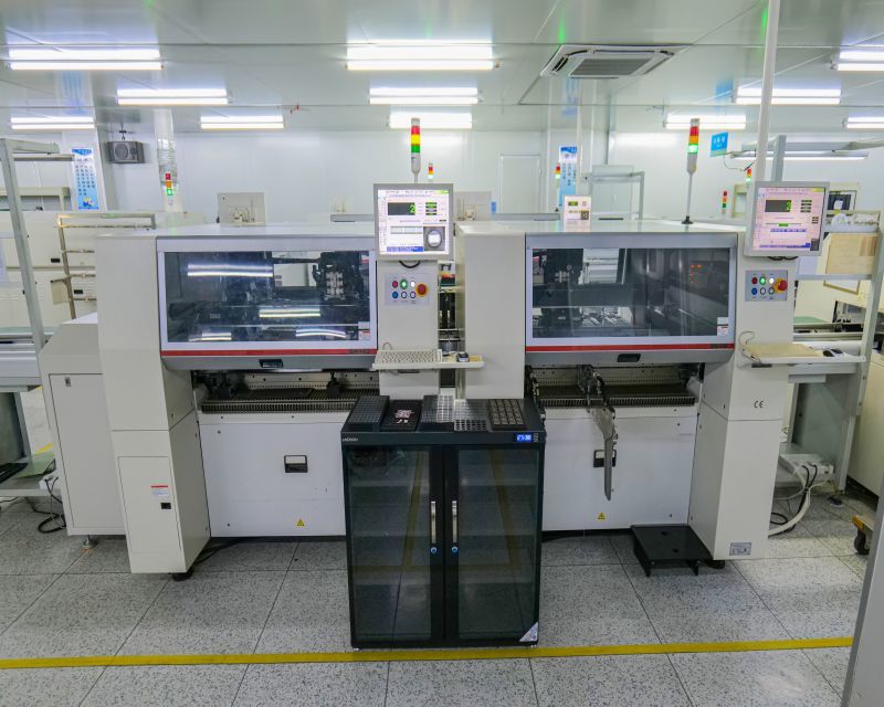
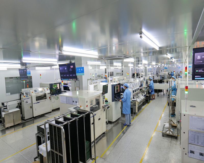
High-end Custom Services: SMT Chip Processing Meets Diverse Industry Needs


(Telephone contact)
Email:
Address: Room 502, Building 1, No. 13, Bohua 4th Road, Huangpu District, Guangzhou City
COPYRIGHT © 2025 Guangzhou Tongsen Electronic Technology Co., Ltd. All rights reserved.