Welcome to Guangzhou Tongsen Electronic Technology Co., LTD. Website!
What are surface mount devices or SMD packages?
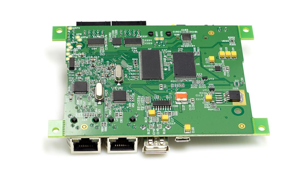
SMT, or Surface Mount Technology, is a new generation of PCB assembly technology. Another PCB assembly technology is through-hole PCB assembly. Therefore, it is actually a technology, not a component.
Whether or not you work in the electronics assembly industry, you've likely heard terms like SMD, SMT, or similar. These are common terms frequently encountered by anyone involved in technology.
Almost all mass-produced electronic products use surface mount technology, but not all components can use surface mount devices (SMD). In SMT, the main component type is surface mount, but THT is also used.
These industry-specific terms can sometimes be confusing. People often ask, "What is SMT?" "What is SMD?" Understanding these terms is crucial for a deeper understanding of the electronics assembly industry.
What is SMD?
SMD stands for Surface Mount Devices. It refers to components using surface mount technology (SMT). Therefore, SMD can also be called SMC, or surface mount component.
SMDs come in various package forms, and most are standardized, making automated PCB assembly more feasible and easier.

Difference between SMD and SMT
What is SMT?
SMT, or Surface Mount Technology, is a next-generation PCB assembly technology. Another PCB assembly technology is through-hole PCB assembly. Therefore, it's a technology, not a component.
SMT is a very popular circuit board assembly technology in the modern electronics assembly industry. The complete SMT process can be divided into five processes: single-sided assembly, double-sided assembly, etc. Production equipment includes solder paste printers, pick-and-place machines, reflow ovens, optical inspection machines, and dispensing machines.
Surface mount technology has high requirements for the environmental conditions of the production workshop. Generally, a dust-free workshop, constant temperature, and low humidity are required. Workshop personnel need to wear dust-free clothing, anti-static shoes, and gloves.
We've discussed SMT in detail. Let's understand what SMD is.
SMD is a surface mount component suitable for SMT PCB assembly. It mainly includes rectangular chip components, cylindrical chip components, composite chip components, and irregularly shaped chip components, such as CHIP, SOP, SOJ, PLCC, LCCC, QFP, BGA, CSP, FC, and MCM.
Advantages of SMT
SMT technology achieves high density, high reliability, miniaturization, low cost, and automated production of electronic product assembly.
SMT has high assembly density. Because electronic products can be designed smaller and lighter, the size of the circuit board is also reduced. The volume and weight of SMT components are only about one-tenth that of traditionally used plug-in components. After SMT, the volume of electronic products is reduced by 40%~60%, and the weight is reduced by 60%~80%.
High reliability, strong vibration resistance, and low solder joint defect rate.
It has excellent high-frequency characteristics and can reduce electromagnetic and radio frequency interference.
Easy to automate, improving production efficiency, saving materials, energy, equipment, labor, and time, and reducing costs by 30%~50%.
Using SMT technology, we can design more advanced products and apply electronic products to more fields, such as CPUs and smartphones.
SMT is more suitable for mass production because SMT technology replaces manual plug-in operations with automation, using pick-and-place machines to mount electronic components. Therefore, it is more suitable for mass production of high-quality products, and the quality is more stable.
Characteristics of SMD
The main characteristic of SMD is that its shape and structure are different from traditional plug-in products.
SMDs are small, lightweight, have short or no leads, and are highly reliable. They are characterized by impact resistance, vibration resistance, and interference resistance.
SMDs are easy to achieve semi-automatic and fully automatic assembly, and most SMDs use reel, tube, or tray packaging, which helps improve assembly efficiency.
Due to their small size, SMDs can achieve high-density assembly, and their solder joint failure rate is less than ten parts per million.
Using SMD mounting can increase the operating frequency of electronic circuits to 3000MHz (500MHz for through-hole mounting).
It can effectively reduce parasitic parameters, which helps improve the high-frequency characteristics and operating speed of the equipment.
SMD products have high dimensional accuracy and good consistency.
SMD Technologies Used
(1) Pressing Process Technology
In the past, there were three main process methods:
Mechanical punching process (dry method)
Overlapping printing process (wet method)
Internal connection process (wet method)
However, these three process technologies have drawbacks and cannot effectively produce smaller and finer chip components.
Now, the mechanical punching connection process has been greatly improved. Using laser punching, close-fitting printing, and automatic micro-hole injection molding technologies, the hole diameter is reduced to 50μm, the positional accuracy is ±20μm, the printing line width and spacing are both 50μm, and the positional accuracy is ±10μm. This allows for the production of smaller and more refined chip components and LTCC passive integrated components.
(2) Ultrathin Dielectric Layer and Nanoparticle Technology
The current capacitance of chip multilayer ceramic capacitors (MLCCs) has been increased to 100μf and has been put into practical use. This is thanks to the support of ultrathin dielectric layer and nanoparticle technology. The thin and uniform dielectric layer thickness shows the current development level of ultrathin dielectric layer technology.
In order to make the thickness of the ceramic dielectric layer reach 1μm, the particle size of the ceramic powder must reach the nanometer level. Metal electrodes must replace Ag/Pd, the number of layers must be increased to hundreds, and the cost must also be considered. Therefore, the development of reduction-resistant nano-ceramic powder has become a key issue. Significant progress has been made in this area both domestically and internationally.
(3) Thin Film Technology
In previous years, thin film technology was mainly used to manufacture thin film circuits represented by microwave integration. The cost was high, and the production scale was small.
In recent years, thin film manufacturing technology has made significant progress. In addition to traditional physical methods, chemical methods have also played a significant role, leading to low-cost, large-scale production. Chip components manufactured using this technology are characterized by their small size, excellent high-frequency characteristics, and ease of integration.
(4) Semiconductor Microelectronics Technology
In the last two decades of the 20th century, semiconductor microelectronics technology has seen astonishing advancements, progressing from micrometer to sub-micrometer, and then to deep sub-micrometer levels. It offers high productivity, low cost, and high reliability. Currently, domestic production levels have reached 0.18 micrometers. In contrast, the development of passive component manufacturing technology has not been as fortunate. In recent years, passive component manufacturing has begun to borrow and adapt semiconductor microelectronics technology, a wise move that has yielded quick results.
Previous
RECOMMENDED NEWS
High-end Custom Services: SMT Chip Processing Meets Diverse Industry Needs


