Welcome to Guangzhou Tongsen Electronic Technology Co., LTD. Website!


Printed Circuit Board Basics: From Design to Final Product
While PCB design and manufacturing can be summarized as schematic capture, PCB layout, and circuit board manufacturing and assembly, the details of each step are quite complex. We will introduce some more specific aspects of each step here.
Key Points
Defines two main concepts for board design and production: grade and construction.
Layout department responsibilities overview: library part generation, layout, and routing.
Each task from schematic/design document to manufacturing file is more meticulously performed.
Electronic devices are ubiquitous in the modern world. Whether it's a device silently monitoring vital signs or a smartphone constantly emitting notifications, at the heart of their design is the PCB circuit board. Over the years, the printed circuit board manufacturing industry has continuously evolved to meet the ever-growing demand for newer, faster, and more complex electronic circuits. A discussion of the design and processes involved in designing a PCB circuit board could fill a library, but here we will provide a surface-level introduction to the fundamentals.
What is a Printed Circuit Board?
A printed circuit board is a rigid structure containing a circuit composed of embedded metal surfaces (called traces) and larger areas of metal (called planes). Components are soldered to metal pads on the board, which connect to the board circuitry. This allows components to interconnect. A board can consist of one, two, or multiple layers of circuitry.
Circuit boards are made using a dielectric core material with poor conductive properties to ensure pure circuit transmission and are separated by additional metal and dielectric layers as needed. The standard dielectric material used for circuit boards is a flame-retardant composite of woven fiberglass cloth and epoxy resin, known as FR-4. The metal traces and planes of the circuit are typically made of copper.

Printed circuit boards have a variety of uses. A notable characteristic of a PCB is its grade—1, 2, or 3. The grade of a PCB indicates its overall reliability and design quality.
Class 1 circuit boards refer to consumer electronics.
Class 2 circuit boards are suitable for equipment where high reliability is important but not critical. These devices will minimize failures.
Class 3 circuit boards represent stringent manufacturing standards for PCBs. In short, if a Class 3 circuit board fails, life is immediately threatened—for example, circuit boards on aircraft.
Types of Printed Circuit Boards
Generally speaking, circuit boards can be categorized into three types: rigid circuit boards, flexible circuit boards, or metal core circuit boards.
Rigid boards are typically the vast majority of boards a designer will encounter, where the layout of the circuit board is contained within a rigid substrate created through a high-temperature, high-pressure lamination process. The common material for these boards is FR-4. However, depending on the specific needs of the design, it can be modified to emphasize or otherwise improve certain characteristics of the board.
Flexible boards are made from a less rigid material, allowing for greater deflection. This material has a feel reminiscent of film, and the thickness of the board is typically far less than a standard rigid board. While flexible boards are already widely used, there is hope that it will lead the next step in wearable technology and eliminate the planar limitations inherent in rigid board devices.
Metal core PCBs are an offshoot of rigid board design that features enhanced heat dissipation capabilities to protect sensitive circuitry across the board. This design can serve as an option for high-current designs to prevent thermal wear and failure.
Wherever there is controlled electromagnetism, printed circuit boards are the foundational infrastructure that sustains it. Of course, circuit boards don't appear out of thin air—their design and manufacture is itself a massive engineering undertaking.
Printed Circuit Board Design Process
Before a printed circuit board can be manufactured, it must first be designed. This is done using PCB circuit board design CAD tools. PCB design falls into two main categories: schematic capture, used to create the circuit connections in a diagram, and then PCB layout, used to design the actual physical circuit board.
Developing a CAD Parts Library
One step is to develop the CAD parts library needed for the design. This will include schematic symbols, simulation models, packages for PCB layout, and step models for 3D printed circuit board visualization. Once the library is ready, the next step is to create a logical representation of the circuit on the schematic. CAD tools are used to place symbols on the schematic and then connect them to form the circuit.
Simultaneously, circuit simulation is performed to verify that the design will work as intended. Once these tasks are complete, the schematic tool will send its connectivity data to the layout tool.
Layout
In the layout aspect of PCB design, the schematic connections are received and processed as nets that connect two or more component pins. After an outline of the intended board shape is displayed on the screen, the layout designer will place the component packages in their correct locations. Once these components are organized in an optimal manner, the next step is to connect the nets to the pins by drawing traces and planes between the pins. The CAD tool will have built-in design rules to prevent the traces of one net from contacting another net and control many other widths and spaces needed to complete the design. Once the routing is complete, the design tool will again be used to create manufacturing drawings and output files that the manufacturer will use to build the board.
The design and manufacture of a circuit board is a step-by-step process: schematic creation and simulation, setting up the PCB design grid and DRC, component placement, PCB routing, power planes, and finally assembling the BOM and building the board. The next phase of the design will focus on these steps.
How is a Printed Circuit Board Made?
While the design and manufacture of a PCB can be summarized as schematic capture, PCB layout, and board manufacturing and assembly, the details of each step are quite complex. We will cover some of the more specific aspects of each step here.
Creating the Schematic
Before beginning the design of the circuit board using CAD tools, it is necessary to ensure that the library parts design is complete. For the schematic, this means creating logical symbols for the parts that will be implemented; resistors, capacitors, inductors, connectors, and integrated circuits (ICs).
Once these parts are ready, the first step is to organize them onto the schematic drawing in the CAD tool. After the parts are roughly placed, lines representing the connections between the schematic symbol pins can be drawn. These lines are called nets, and they can represent a single net or a group of nets for memory or data circuits. During schematic capture, it is necessary to move the process parts as needed to create a clear and easily readable schematic.
Circuit Simulation
After organizing the components and nets on the schematic, the next step is to verify that the circuit works as expected. To verify this, use circuit simulation in a simulator program with integrated circuit emphasis tools. These tools allow PCB engineers to test the circuits they are designing before building the actual hardware. Therefore, they can save time and money, making these tools an important part of the PCB design process.
CAD Tool Setup
The design tools used by PCB designers have a variety of different functions, including the ability to set design rules and constraints that will prevent different nets from overlapping while maintaining the correct distance from different objects. Designers can use a variety of other auxiliary tools, such as a design grid, which helps place components and routing in a neat and orderly manner.
Component Placement
After correctly setting up the design database and importing net connection information from the schematic, the next step is the physical layout of the circuit board. One step is to place the component packages within the circuit board outline in the CAD system. The net connections of each package will be displayed as a "ghost line" image to show the designer which components they connect to. While placing these components for optimal performance, it is also important to pay attention to connectivity, overheating and electrical noise areas, and other physical obstacles (such as connectors, cables, and mounting hardware), which is a task that designers will gain through experience. The requirements of the circuit itself are not the only constraints: designers must consider placing components so that manufacturers can assemble them in the best way.
PCB Routing
Once the components are placed, it's time to connect the nets. This is done by converting the rubber band net connections into drawn traces and planes. CAD tools contain many features that enable designers to do this, including some automated routing features that can save a significant amount of time. Care must be taken during routing to ensure that the length of the nets is suitable for the signals they are carrying and to ensure that they do not pass through areas with excessive noise. This can lead to crosstalk or other signal integrity issues that will reduce the performance of the built board.
Ensure Smooth PCB Return Current Paths
Generally, each active component (IC and other related components) on a circuit board needs to be connected to the power and ground nets. This can be easily achieved by filling these components with solid planes that can be utilized on the area or layer. However, designing power and ground planes is not as simple as it seems. These planes also bear the important task of returning the signals routed through the traces. If there are too many holes, cuts, or cracks in the plane, it will cause these return paths to generate a lot of noise and reduce the performance of the PCB.
Final Rule Check
After completing the component placement, routing, power, and ground layers, your PCB design is nearing completion. The next step is to perform a final rule check and set the different text and markings that will be silkscreened on the outer layers. This will help others locate the components and mark the name, date, and copyright information on the board. At the same time, it is necessary to output drawings that will be used in the manufacturing process to manufacture and assemble the final circuit board. PCB designers will also use their tools to estimate the cost of building the circuit board.
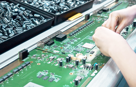
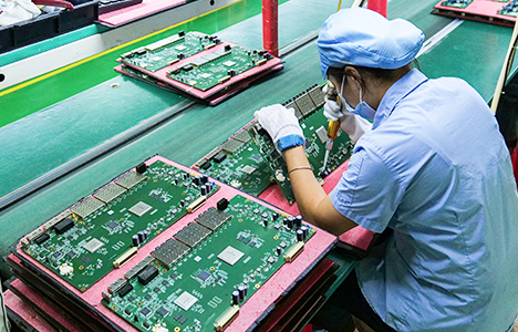
At this point, the circuit board is ready for assembly, one step is to send the output data file to the factory. This process involves etching all the traces and planes onto different metal layers and pressing them together to produce a bare board ready for assembly.
At the assembly factory, the required components are loaded onto the circuit board, and different soldering processes are used depending on the type of components used. The board is then inspected and tested, and the final product can be shipped.
Using PCB Tools for High-Quality Design
The manufacturing and assembly process of printed circuit boards is precise and demanding. In order to manufacture a circuit board so that its circuits can provide the required performance, the manufacturer needs precise design data to work with.
PCB circuit board design tools must have the features and functions needed to create complex designs. This includes specialized functions that help route complex traces for high-speed circuits and design rules that easily set clearances between specific areas. It also includes having optimal simulation tools to simplify your schematic capture process and providing a rich library of parts for you to use. The good news is that there are already available PCB design tools that can handle the level of design expertise we've been discussing.
RECOMMENDED NEWS

High-end Custom Services: SMT Chip Processing Meets Diverse Industry Needs


(Telephone contact)
Email:
Address: Room 502, Building 1, No. 13, Bohua 4th Road, Huangpu District, Guangzhou City
COPYRIGHT © 2025 Guangzhou Tongsen Electronic Technology Co., Ltd. All rights reserved.